Lab 8: - ECE 421L
Final Project Part I
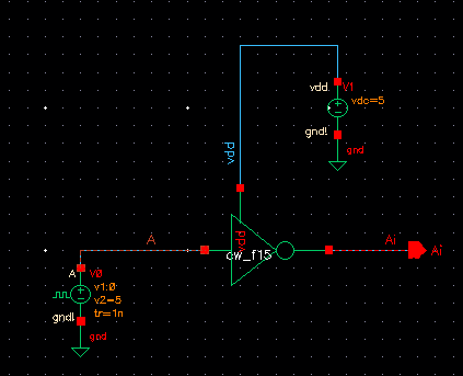 Here is my test circuit. I instantiated my Inverter symbol
and ran a transient simulation. Results are seen below.
Here is my test circuit. I instantiated my Inverter symbol
and ran a transient simulation. Results are seen below.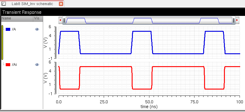
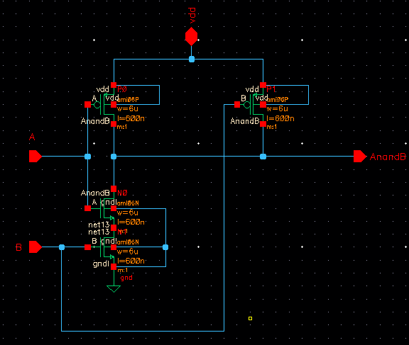
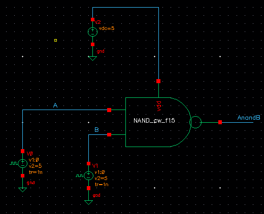 For this simulation I also did a transient analysis. You
can see by the output below that the NAND gate is working just as
expected it should.
For this simulation I also did a transient analysis. You
can see by the output below that the NAND gate is working just as
expected it should.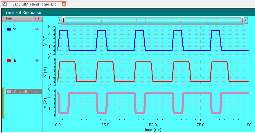
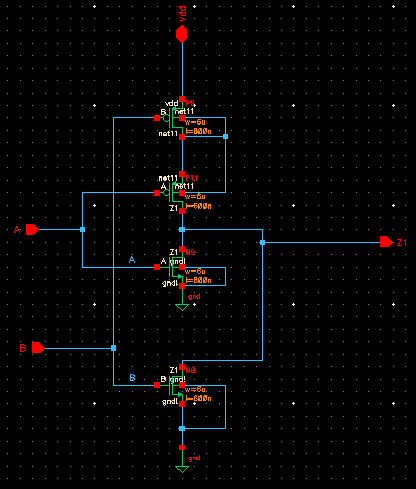
 Using my symbol in a simulation circuit here, it ran as expected.
The output below shows a glitch during my A-input High to Low
switching... This can be smoothed out a little bit more with minor
tweaks.
Using my symbol in a simulation circuit here, it ran as expected.
The output below shows a glitch during my A-input High to Low
switching... This can be smoothed out a little bit more with minor
tweaks.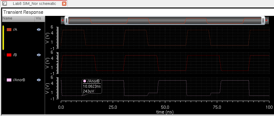
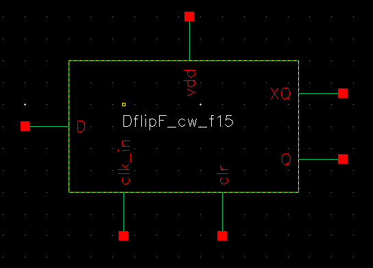 A symbol was made for the Flip Flop in order to help make the Counter circuit more compact and simple.
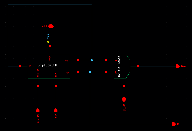
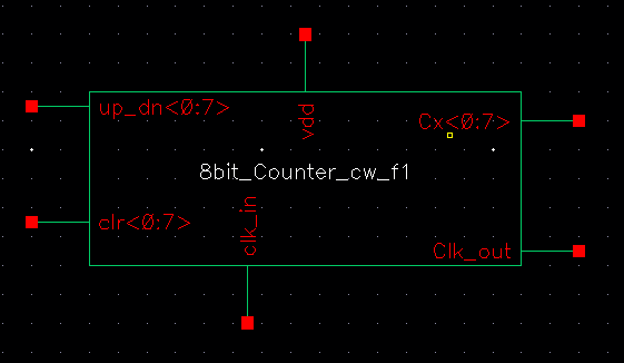 Using the 8-bit symbol I instatiated it into the schematic below
in order to run a simulation to ensure proper operation.
Using the 8-bit symbol I instatiated it into the schematic below
in order to run a simulation to ensure proper operation. 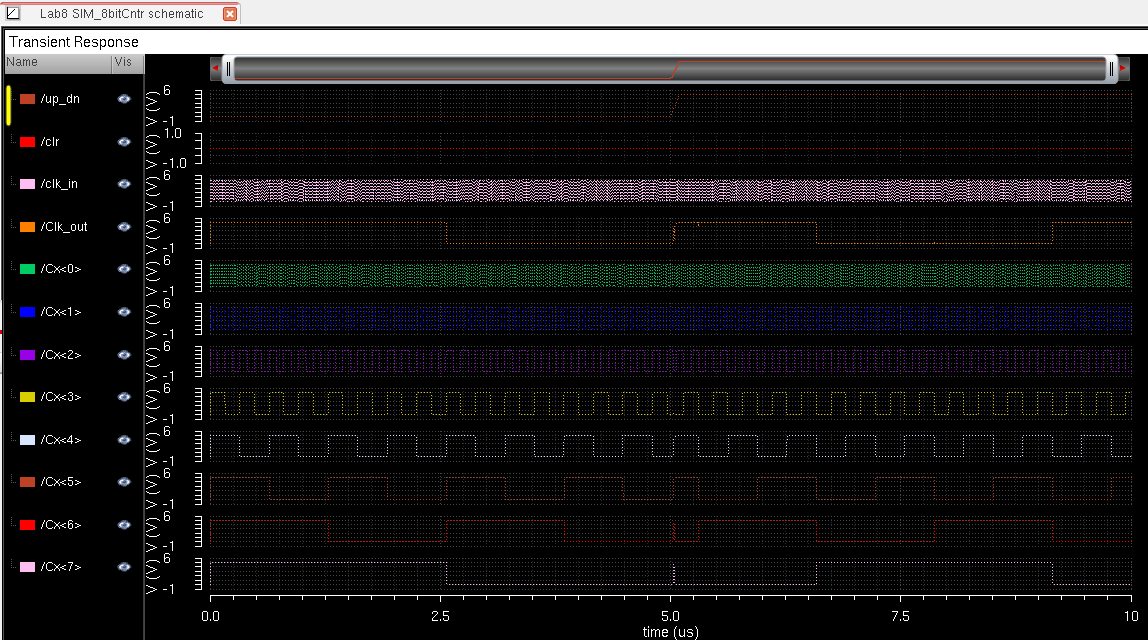
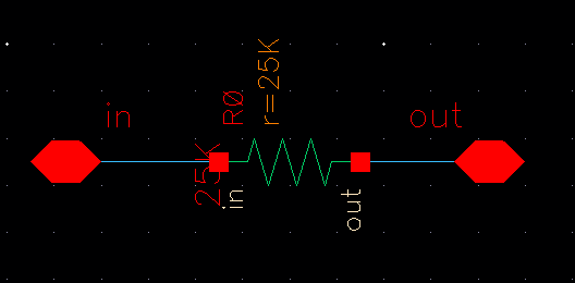
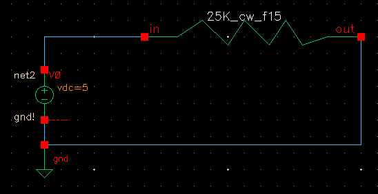 You can see that here we only needed to run a simple DC analysis
to see that the resistor is in fact working properly. Basic Ohms
Law can be used to verify V=I*R. Here I have a 5V input and a 25K
Resistor. You can see that at 0V -> 0A and at 5V -> 200uA.
You can see that here we only needed to run a simple DC analysis
to see that the resistor is in fact working properly. Basic Ohms
Law can be used to verify V=I*R. Here I have a 5V input and a 25K
Resistor. You can see that at 0V -> 0A and at 5V -> 200uA.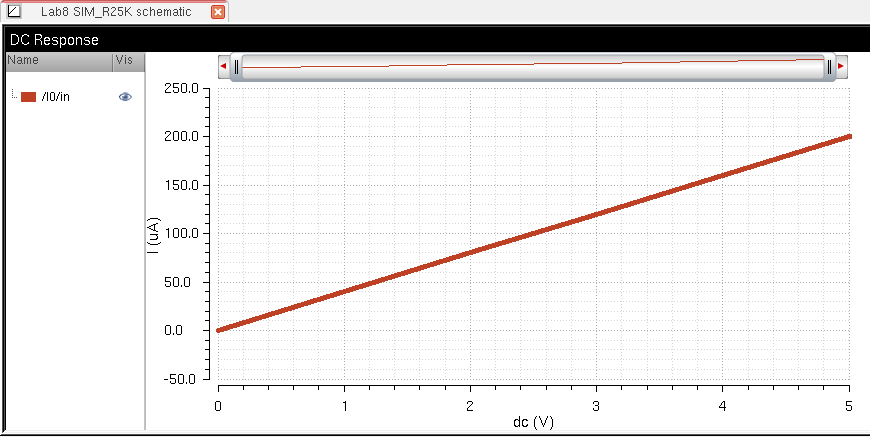
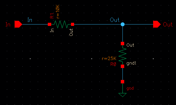
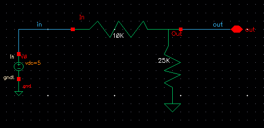 Vout = Vin* [R2/R1+R2]
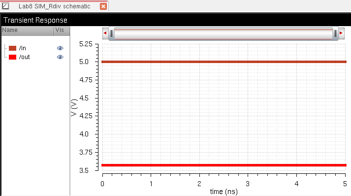 Here, my R1=10K and R2=25K... My results show Vout = 3.57V.
If the resistors were oriented in the opposite arrangement Vout
would be 1.42V.... Either way, the circuit is performing as it should
and as expected.
Here, my R1=10K and R2=25K... My results show Vout = 3.57V.
If the resistors were oriented in the opposite arrangement Vout
would be 1.42V.... Either way, the circuit is performing as it should
and as expected.For the second part of our Lab project we were to layout each of the components that will make up our test chip.
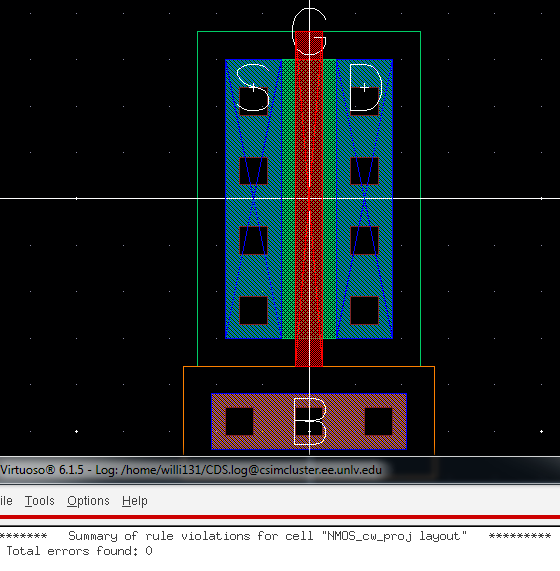
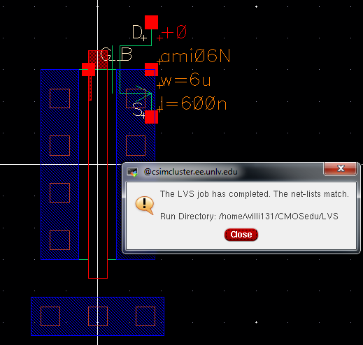
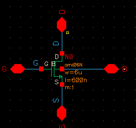
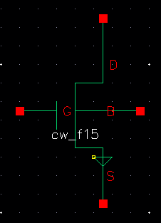
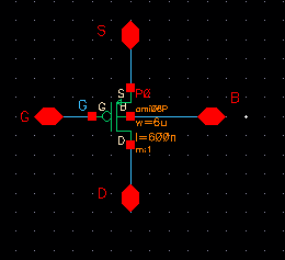
I. NMOS Transistor:
Below is my NMOS layout. As you can see, the source, drain, body and gate are labeled for clarity. Beside the DRCed layout is the successful LVS extraction. This was extracted with the schematic in the first part of the project (above).
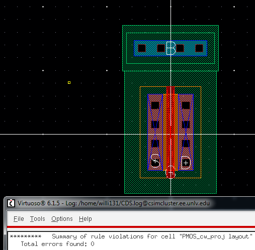
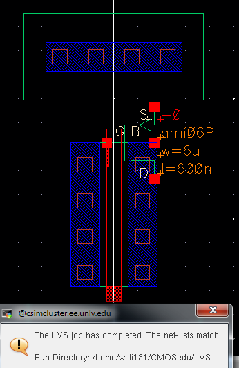
II. PMOS Transistor:
Gate, Source, Drain, and Body labeled below. You can see that the 6u/.6u PMOS layout/extracted matched the netlist with the schematic above as well.
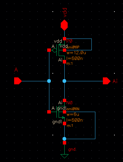
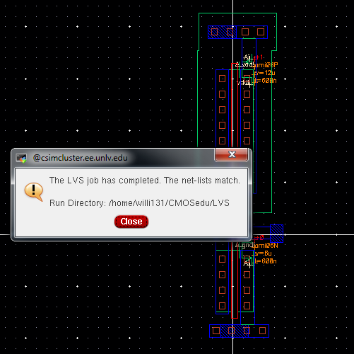
III. Inverter
The layout below, after being extracted was LVSed with the schematic from the first part of the project above. 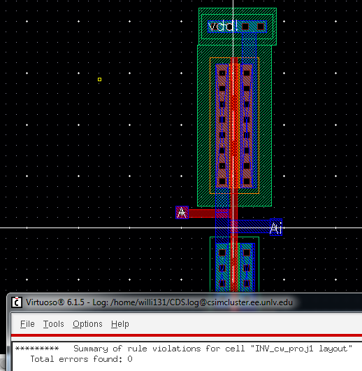
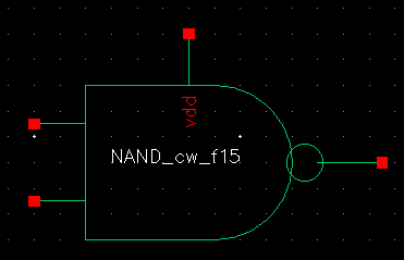
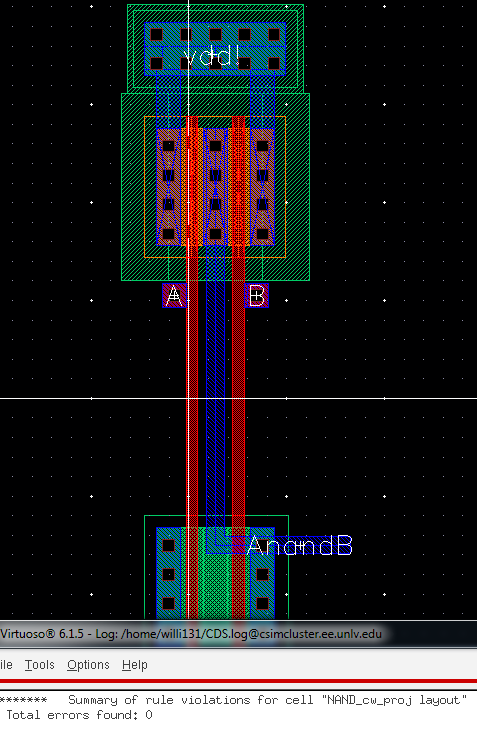
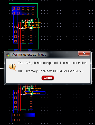
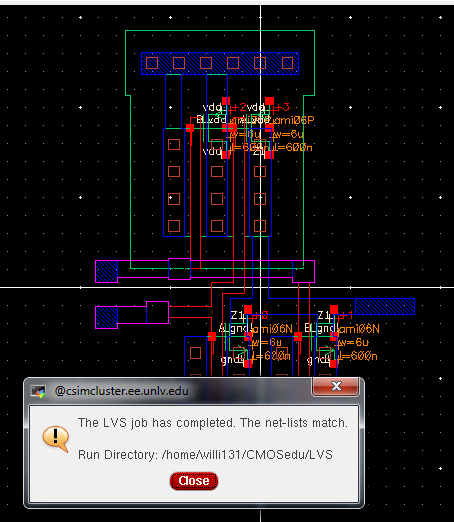
IV. NAND
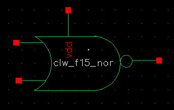
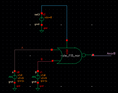
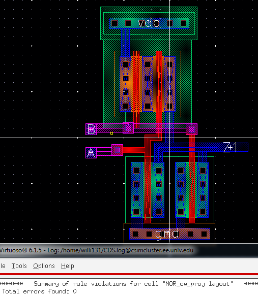
V. NOR
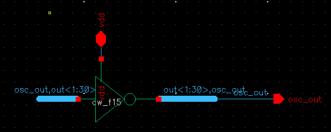
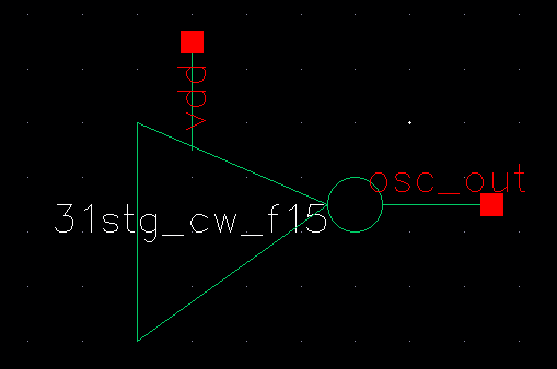
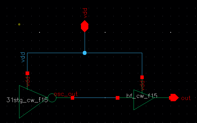
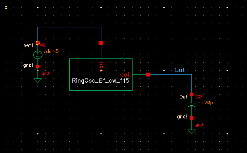
VI. 31-Stage Ring Oscillator with Buffer:
For the Ring Oscillator layout, I layed out each component, checked the DRC and LVS and then put them together.
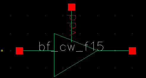
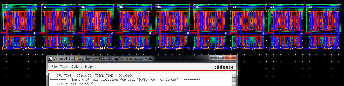
A. Buffer:
Below is the first layout of my buffer... I ended up changing it to correctly have one inverter with the 8 multiplier (as you can see below there is a string of them), and then one with the multiplier of 64. This is better visible in the layout with the Buffer and Oscillator below.
B. 31-stage Ring Oscillator:
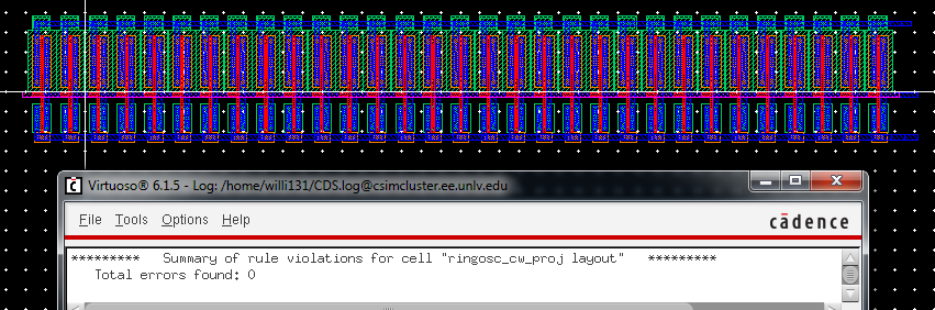
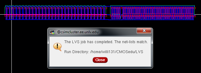
Below is the Ring Oscillator extracted and successfully LVSed with just the oscillator (not including the buffer yet)
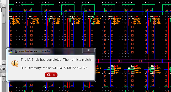
31-stage ring oscillator AND buffer:
Below is the final extracted view and LVS for the ring oscillator and the buffer. You can see here, as mentioned above, that the buffer has one stage with an 8 multiplier, and a second stage with the 64 multiplier.
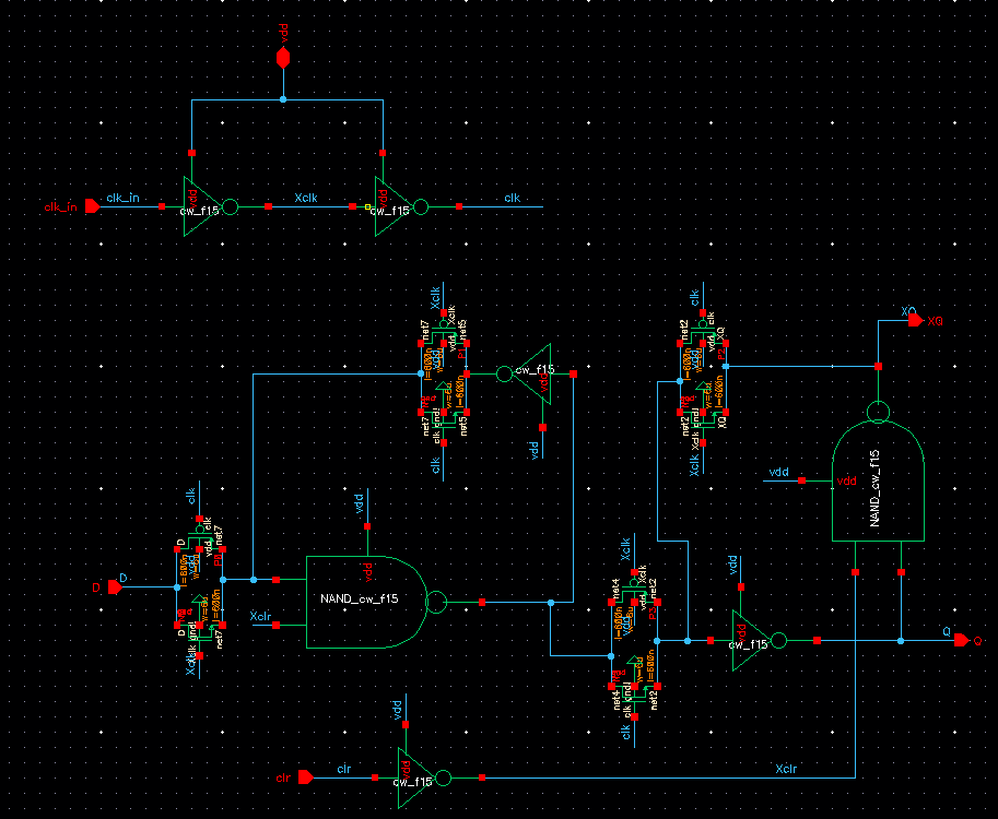
VII. 8-bit Counter:
A. Flip-Flop:
For the 8-bit Counter I layed out each component one at a time, DRCed and LVSed them and then put them all together similar to the way I did my ring oscillator.
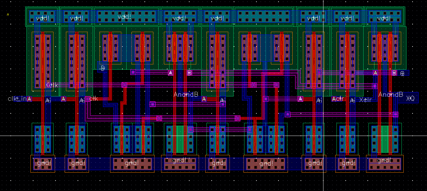
First, I layed out the Flip-flop. Below you can see that the inverters, NMOS, PMOS transistors, and Nand gates were each instantiated and then arranged and connected to their respective terminals. Terminals were labeled for easy layout and connections. This DRCed successfully.
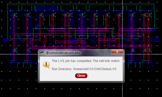
Here, below you can see the the Flip-Flop was extracted and LVSed successfully with the netlists matching *high five* :)
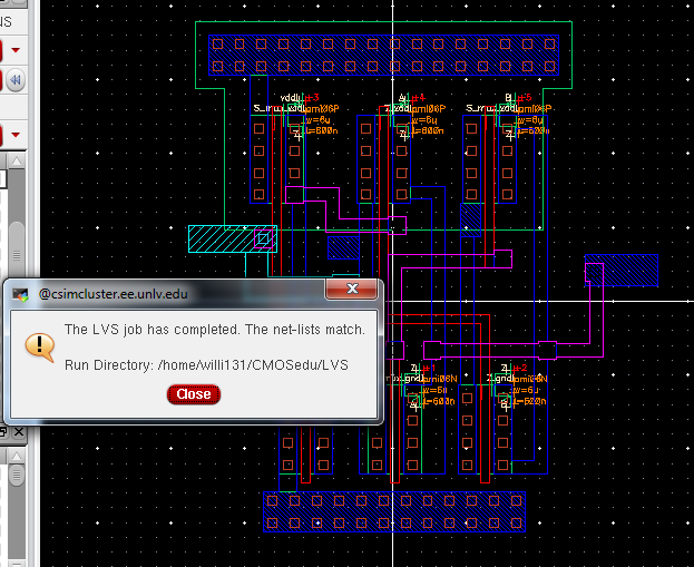
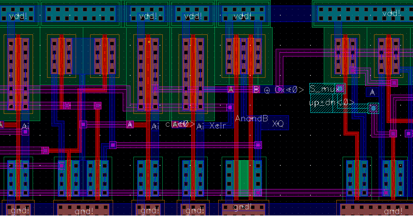
B. MUX/DEMUX:
Next component used in the counter is the MUX. Here, layed out below you can see each terminal as they're labeled for easy following. This was constructed by simply instantiating my NMOS and PMOS transistors and connecting the just like the schematic.
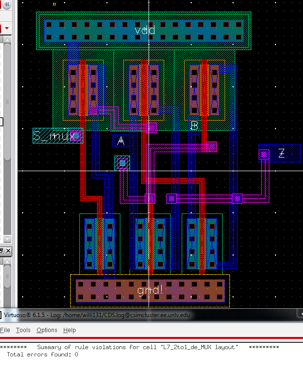
Here is the extracted view of the MUX/DEMUX. As you can see, this was LVSed with the schematic and netlists matched successfully.
C. Counter:
Next, putting the Flip-Flip and MUX together I created a single bit counter. This component, seen below represents only one of the 8 bits that will soon make up our final component...
Below is the extracted and LVSed single-bit counter.
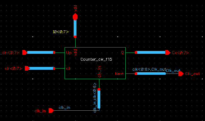
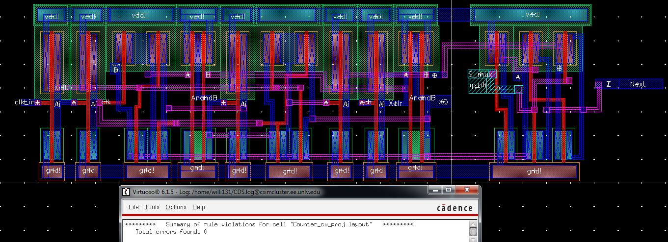
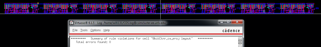
D. 8-Bit Counter
Simply instantiating the counter above into a new layout, I just copied it to build the 8-bit layout seen below. Making the proper connections, and checking design rules, my DRC returned back clean.
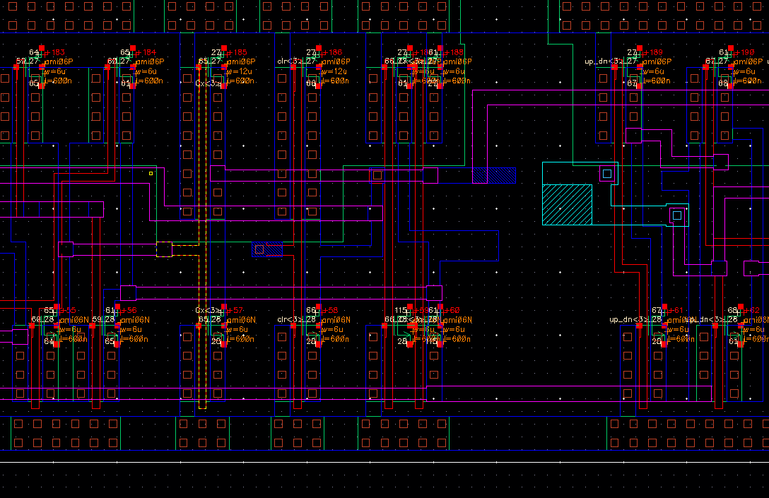
This is a zoomed-in view or the 8-bit counter layout...
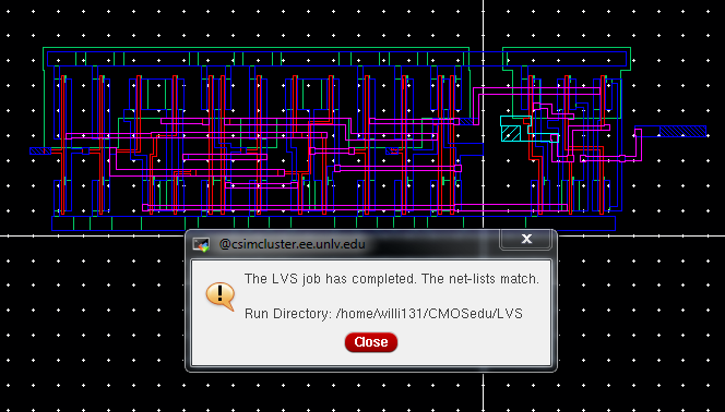
Finally, nexted after the DRC was successful and clean, I extracted the layout as seen below. (zoomed in for easy view)
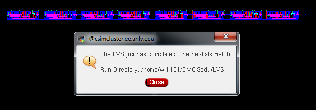
Next, I ran the LVS with the 8-bit counter schematic shown above in the first part of the project report and it returned successful with netlists matching.
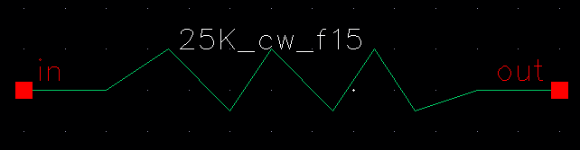
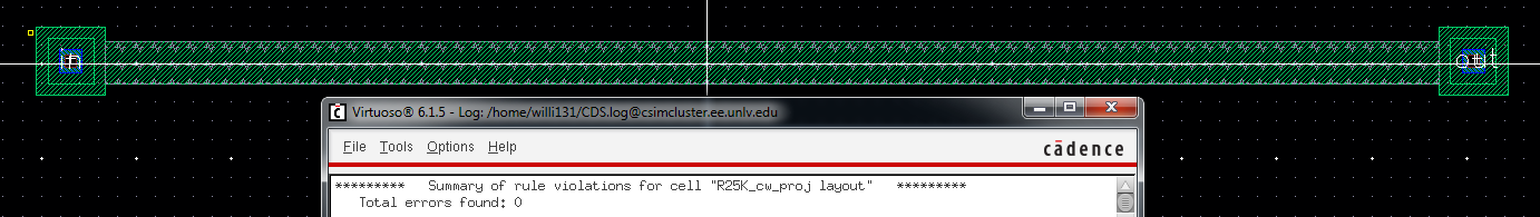
VIII. 25K Resistor:
Below is the 25K resistor layout. I used the n-well to layout the resistor as seen below. DRC and LVS were successful.
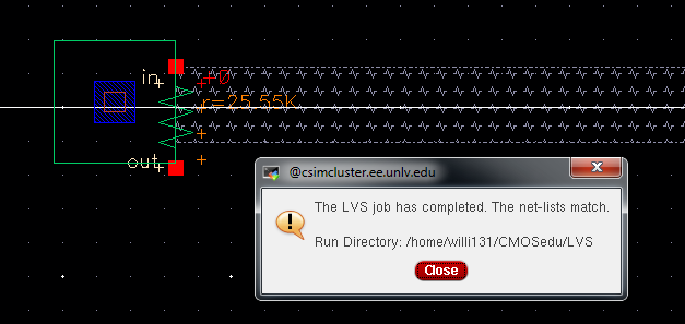
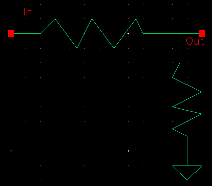
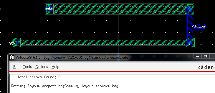
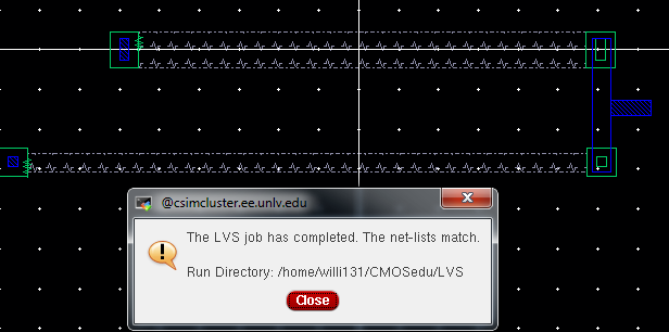
IV. 25K/10K Voltage Divider:
Below is the layout, extracted, and successful DRC and LVS for the voltage divider.
Side Note: For all these layouts, they were all compared with schematics shown in the Part 1 of the project (above). These schematics are the basic, raw schematics that my symbols were created from, not the simulation schematics.
Finally, after arranging groups we will be laying out all the components into a padframe layout in order to get a test chip fabricated. Laying out the components will be simply instantiating them into the padframe layout and making the connections to the pads. For this project each component will have their own power supply (vdd) connection. This will be simply sorted out by naming each vdd on the schematic's pins as vdd<1>, vdd<2>, and so on.. Then all of the components will have the same global Ground (gnd!). Arranging things this way will help prevent any issues with one particular component/circuit effecting any of the other ones on the chip. (ie. in case there is a short vdd-gnd in one circuit, it wont short everything out).
My design directory and all the schematics, layouts, extractions, and sims can be found here. These were also all backed up via email/flashdrive.
Return
to the directory listing of students in EE 421L, Fall 2015
Return to the EE421L
Fall 2015 webpage