
Lab 3 - EE 421L
Pre-Lab
Following up Tutorial 1 from where I left off (until image 25), I went back to the original schemetic and deleted the voltage source and added pins for input and output as seen below.
Then, I created a symbol of the design (Create -> Cellview-> From Cellview) as follows.


Drawing a symbol for this (Create -> Shape ->Line), it looked like this:

Next, I verified that this symbol gevis the same result as the original simulation, so I instanciated it in a new schematic and simulated it.


After that, I then layout the resistive divider, but I first create a layout one 10k n-well resistor.

Since we are working using the C5 process, the sheet resistance is roughly 800 ohms, the minimum width is 12 lambda (3.6u). Aso, the X and Y snapping is 0.15 microns, so every measure should have to be multiple of 0.15. Then,based on the tutorial, a width of 4.5um and a length of 56.1um were used.
Pressing 'r' to draw a rectangle and in the n-well layer specifying the given dimensions, the resistor looks like this:

Make sure to DRC ( Verify-> DRC) the layout and show no errors

Adding two n-tap connections to both ends of the resistor, a rectangle in layer res_id, and pins called L(left) and (rigth), the final 10k resistor will look like this:

Next, let's extract the layout (see below)


The resistance is 10.21k, which is close enaugh to our desired value of 10k.
Now, let's layout the resistor divider. Two 10k n-well resistor were instantiated. Then, I added input pin 'in', output pin 'out', and ground 'gnd!' in layer metal 1. (see below)

After verifying that DRC shows no errors, extract the layout.

Now, it is time to LVS both the extracted layout and schematic. On layout select Verigy -> LVS. (see below)

After the LVS succeded, verify that the netlists match as follow.

----------------------------------------------------------------------------------------------------
----> For the 10k layout, try a resistor length of 55.2um
Post Lab description: During this lab, we layout our 10-bit DAC that was designed and simulated in Lab 2.
Since the 10-bit DAC layout was to be LVS with the circuit desgined in Lab 2, I copied the Lab 2 contents into a new library called "Lab 3".
This non-ideal 10-bit DAC was designed using 10k resistors, so the main component to layout my DAC is the layout of a 10k resistor, which was exactly the resistor developed in Tutorial 1 (add link).
The resistor was designed according to follwing formula:

Let's define the the sheet resistance (R_square), length (L), and width (W).
Since we are working using the C5 process, the sheet resistance of an n-well is approximately 800 ohms. Also, the minimum width of a n-well is 12 lambda, where lambda is 300nm accoriding to SCMOS_SUBM, making the minimum width equal to 3.6um. Although width and length should be larger than 3.6um, the defualt spacing used in CDS is 0.15um, so whatever length and width we choose, it must be multiple of 0.15um.
Then, a 56um length and a 4.5um width, which both are multiples of 0.15um, would generate roughly a 10k resistor (see below).

Now, we can layout the 10-bit DAC based on the shematic shown below.


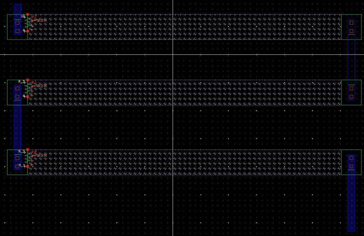
First, I layout the cells that are connected to each one of the 10 pins (see above, right), so a layout cellview was created for the cell "2R_R_10k".


This "Bit_Res_10k" cell uses 3 10k resistor and pins (see above, left).
 put link for bigger view
To verify that the dimensions are correct, we can measure them using the ruler tool by pressing 'k'. To delete rulers, press 'shift + k'.
One have to make sure that I/O type of each pin matches the ones in the schematic (input, output, or InputOutput).
DRC the layout and make sure that no errors have been encountered. Then, extract the layout.
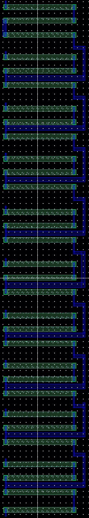
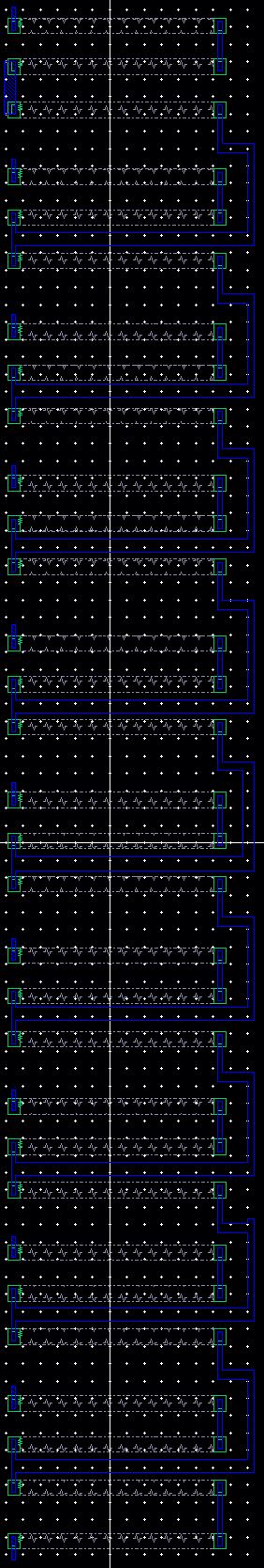
Next, the layout for the cell "my_10bit_DAC" will be created. The "2R_R_10k" layout is instantiated 10 times, one under the other, i.e. the resistor are stacked ( see below).
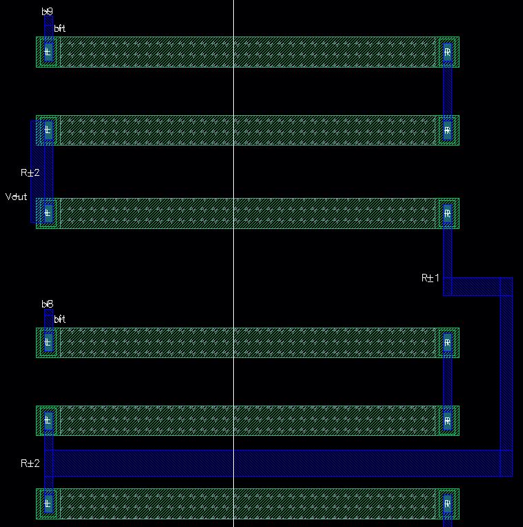
Pins for each bit and ground will be added on metal 1 layer making sure that I/O type matches the corresponding schematic (see below for a zoomed view).
Again, DRC the layout showing that there is no errors and then extract it.
Now, it is time to LVS (Layout vs Schematic) my layout (Create-> LVS). After pressing Run, a dialog box pop-up showing the netlists match! I pressed ouput to verify how both netlists match.


All the mentioned cell files can be found and downloaded in the following link: