
Lab 2 - EE 421L
First of all, I am to back up all my work from the lab in case of failure.
I then donwloaded lab2.zip to my desktop. After that, I logged into my MobaXterm account, and upload the files into my CMOSedu directory.
Once all the contents of the zip file are extracted, I added to my cds.lib file in my directory the following definition:
DEFINE lab2 $HOME/CMOSedu/lab2

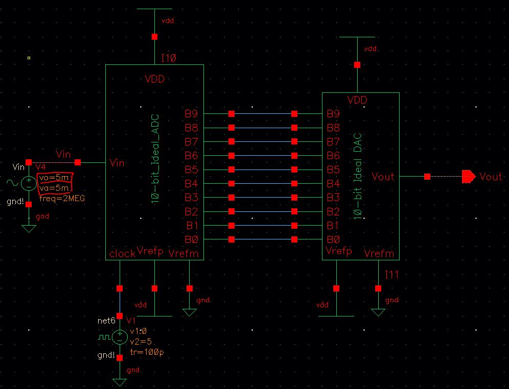
Then, I could start Cadence Virtuoso, and open the corresponding schematic for this 10-bit ADC and DAC, which is sim_ideal_ADC_DAC.

I then obtained the picture shown below. Immediately after, I proceded to launch the ADE, loaded state, an pressed the green button to simulate.
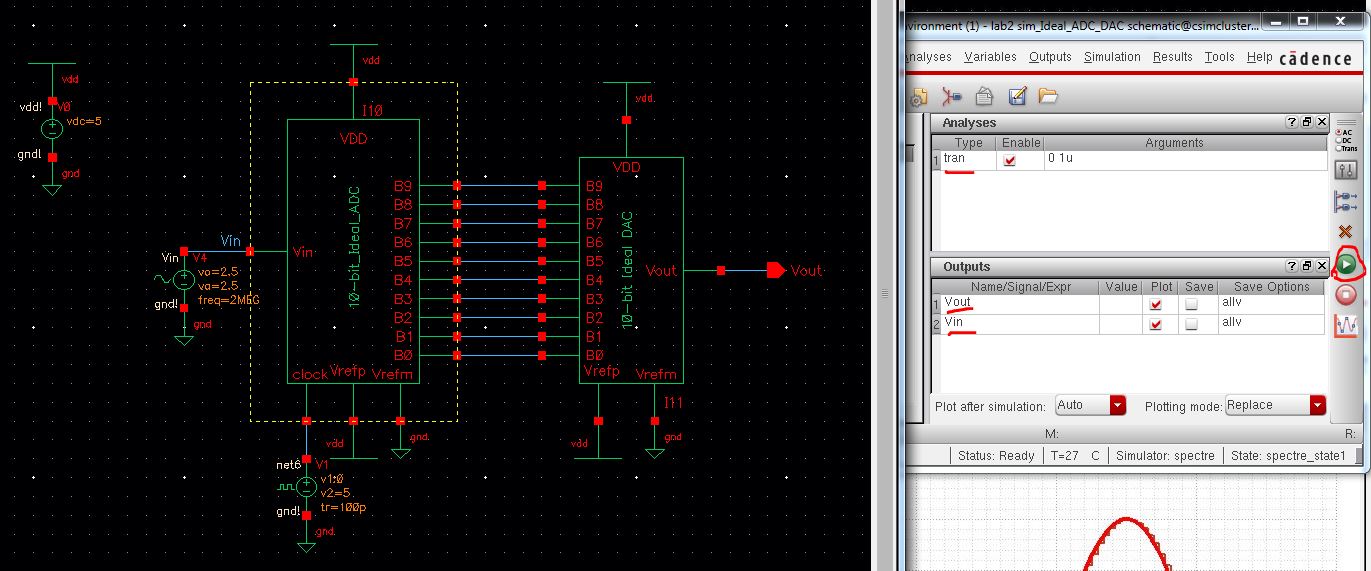
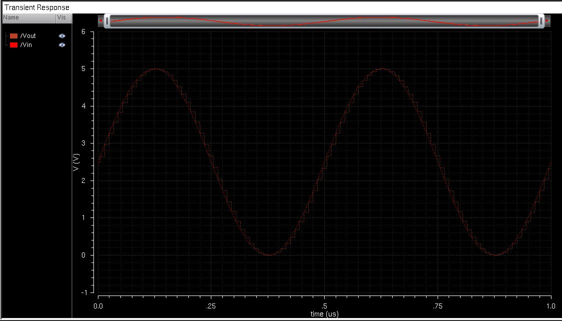
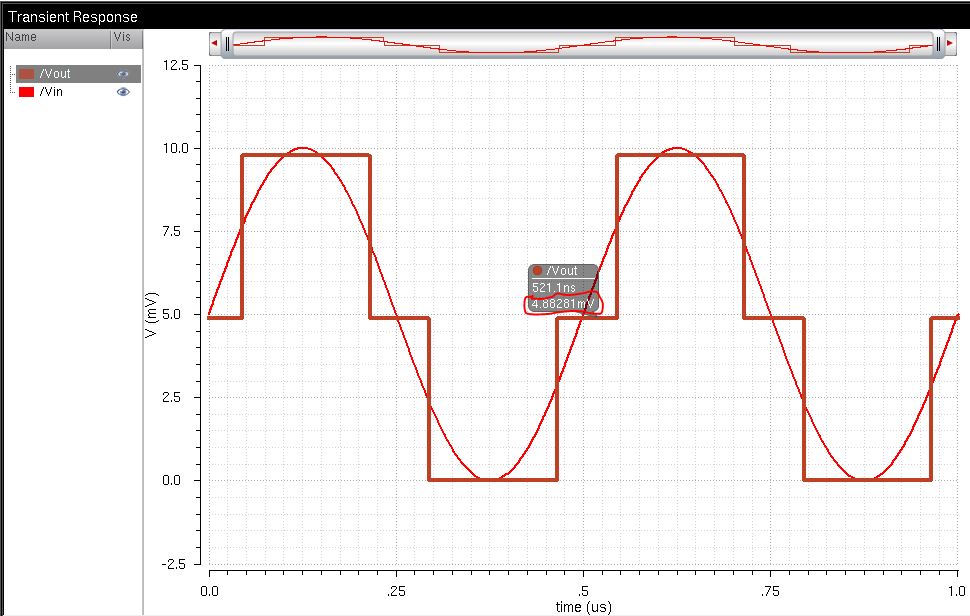
For a better understanding of the graph (above), I changed the background and adjusted the line thickenss selecting the "Trace Properties..." option (right click the plot).

Part 2 - Discussion and simulation of different values
For this case, I changed the input values of the design and then analyse the output results in the simulation.
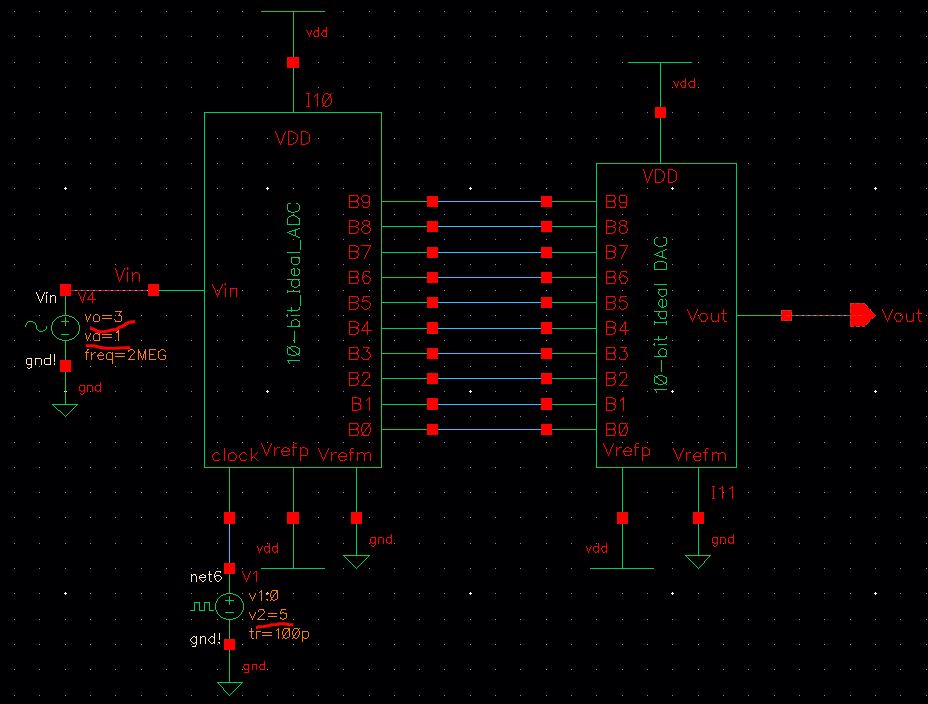
If I change the amplitude to 1V and offset to 3V, I expect the simulation input and output to go from 2V and 3V (see below)

However, if I change the offset to 0V, the analog input would go from -1V to 1V, but the digital output would range between 0 to 1V due to the circuit is set to allow values ranging between 0v to 5v., as shown below

Refering to the two simulations shown above, it is seen that the analog input is converted to a digital output, which means that it is represented in discrete values (binary) over the range 0v to VDD=5v. In the ADC, the conversion involves quantization of the input over a minimum range set by the least significant bit (LSB), i.e. it samples the input and convert it into 10 bit binary number. In the DAC, the input is the 10 bit number and the output is the analog singal representation of it that can be plotted.
Part 3 - How to determine the least significant bit (LSB)
The LSB accounts for the minimum voltage change in the input that can be plotted in the output as a discrete value, i.e. it gives the number of discrete values over a range of analog inputs. Hence, I calculated the minimum range based on the set values of the circuit (5V and 10bits).
Due to this is a 10 bit circuit, only 2^10=1024 values are possible over the range VDD=0v to 5v.
The following formula will be used: LSB=VDD/(2^n), where n represents number of bits, n=10.
What this formula does is dividing the range of 5v into the number of possible change levels
-> LSB=5v/1024=4.88mV, and this is minimum voltage change level.
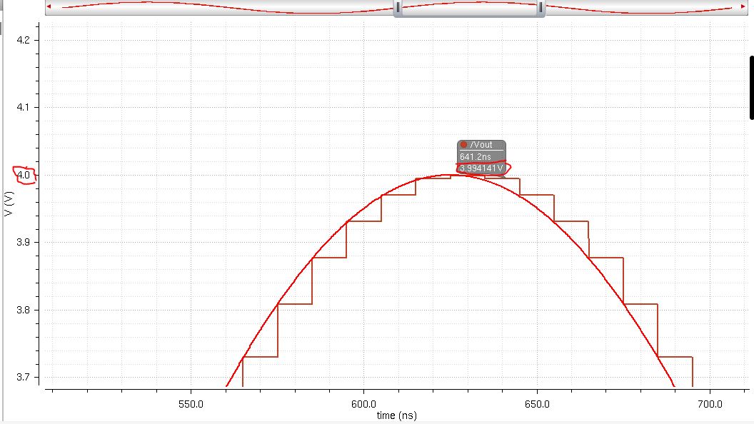
As seen in the plot above, the minimum voltage change is 4.8828 mV between 4V and 3.994141V; a value that is close enaugh to hand calculations.
However, if I set the input voltage to this minimum voltage change (LSB), assuming 5mV, as shown above, we can clearly obtain the exact LSB as an discrete output (see below).
At the end, I backed up my prelab 2 in my flashdrive and google drive.
----------------------------------------------------------------------------------------------------------------------------------------
Post Lab description: During this lab I was to design, implement, and simulate our own 10 bit Digital-to-Analog
Converter (DAC) using 10k n-well resistors based on the follwing topology:

Part 1 - Designing 10-bit Digital-to-Anaolg Converter (DAC) using 2R and R resistors
To begin with, I first designed a new cell (see below left) called "2R_R_10k" that implement the 2R and R resistor in parallel (2R as two R resistors in series). This schematic is used as a voltage divider. Based on this, after pressing 'check and save', I then created a symbol (see below right), which was named "Bit_Res_10k."


Using this symbol, in the following picture, I created a new cell called "my_10bit_DAC" implementing the resistors in series and finally connecting them to a 10k resistorto ground. I labeled each input in descending order as bits called (b9, b8, ..., b1, b0) being the b9 cell connected to a 5v source voltage.

This shecmatic were turned into a symbol called "my_10bit_DAC" in such a way that the 10 input bits were on the left and the output Vout on the right.

Before instantiating this new symbol in the main ideal 10-bit ADC and DAC, I first simulate it by grounding the pins b8 to b0 and connecting b9 to a pulse source (see below)

The delay of the simulation was to be measured and compared with actual caluculations. To do this, I loaded the schematic with a 10pF capacitro, as state in the lab. 0.7RC was ued to predict the delay, but the equivalent resistance of the circuit needs to be found.

As we learned during the last lab, by combining the resistors in parallel and series for any given number of bits configuration, the equivalent resistance is R (see above for the first 3-bits).
Then, 0.7RC=0.7x10kx10p=70ns. As seen below the simulation matches my predicted result.

Part 2- Implmenting my 10-bit ADC and DAC
First, I copy the original schematic to a cell "sim2_Ideal_ADC_DAC." I then deleted the original 10 bit DAC a placed my 10-bit DAC as follows:

After clicking "check and save," I simulated the schematic and the following was obtained:

It seen that the output results worked as expected; the same as the first ideal 10-bit ADC and DAC.
Next, I simulated my schematic under different loads (R, C, and R/C).
- When driving a 20k resistor load, it should behave as a voltage divider. In this case, Vout=Vinx(2/3).


As seen in the simulation above, we can still see the sampling behvior of the output; discrete output values for the analog input.
-When driving a 100pF capacitor load, hand calculations for the amplitude show the following:


The capactir adds delay in the ouput, so the output plot looks smoother; similar to the input but shifted. The delay is 0.7xRxC= 7ns.
- When a 20k resistor and 10pF capacitor loads are added, the result is similar as the previous case, but the equvalent resistance is smaller (R=20/3k).


Finally, as required for this lab, when the schematic drives a 10k resistor, as explained above, it works as a voltage divider. For this resitance, the output amplitude is half the input amplitude(Vout=(1/2)xVin). The discrete output values are not affected. There is no delay.


Part 3 - What happens if the resistance of the switches isn't small compared to R
If the resistance of the switches becomes significantly large compared to the R resistor, they would be counted as part of the circuit and considered in our calculations. They would be connected in series to the 2R resistors.
Then,

It would affect the overall resistance of the circuit and for each bit, which is supposed to be the same as stated above. Therefore, the voltage drop on each bit would not be even,i.e. the voltage increment of two consequetive binary number (one bit difference) would be greater as the number increases.
As always, I backup all my work in Google drive, my laptop, and my flashdrive.
