1) 8-bit resettable (with clear) up/down counter
2) 31 stage ring oscillator with a buffer for driving a 20pF off-chip load
3) a NAND gate
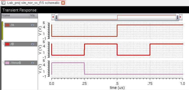
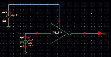
4) a NOR gate
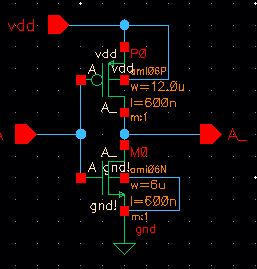
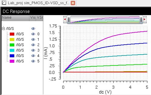
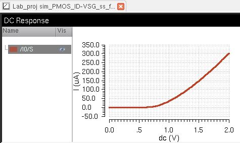
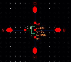
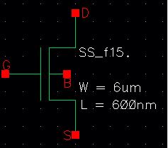
5) a PMOS transistor
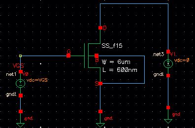
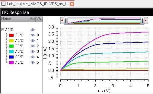
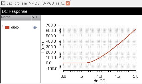
6) an NMOS transistor
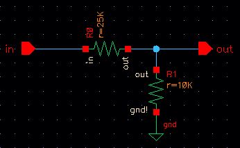
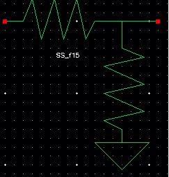
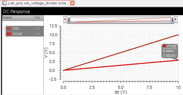
7) a voltage divider between a 25k resistor and a 10k resistor
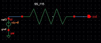
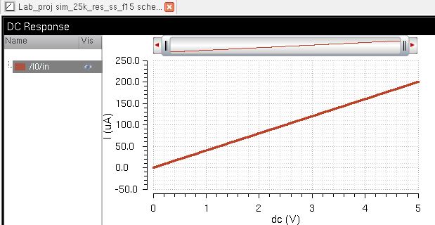
8) a 25k resistor
Report:
1) 8-bit resettble (with clear) up/down counter
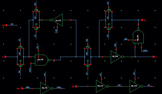
This 8-bit up/down counter is designed with D flip flops. A clear is implemented by the NAND gates in the following schematic. When the clear input is high, a 0 will be transmitted to Q, resetting the flip flop. The clear doesn't have to wait for the rising edge of the clock, hence it is an asynchronous clear.
Note a vdd pin is needed, so that each circuit in the project can be connected to its own vdd pad.
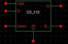
The DFF schematic:
The symbol is created as follows:
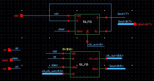
Now, to create the counter from this D flip flop, we will need to have 8 of them, DFF<0:7>, with the clock signal for the second flip flop coming from either Q or QNOT of the previous flip flop. This clock will determine whether the counter is counting up or down.
The schematic and symbol for the DFF register cell are created as follows:
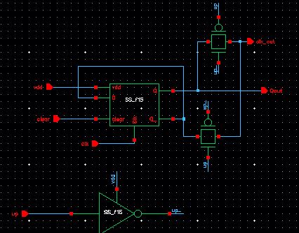
Now, the last flip flop, DFF<7>, will not need to create the clock signal for another flip flop, so we do not need the transmission gates for it. Thus, we use the DFF symbol to create 7 flip flop cells, and add the 8th one without the transmission gates.
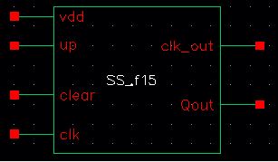
The symbol is created:
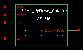
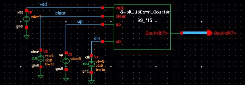
Finally, we can take the symbol for the 8-bit counter and simulate its operation:
Simulation for all 8 bits, counting up (up is 5V), then clearing:
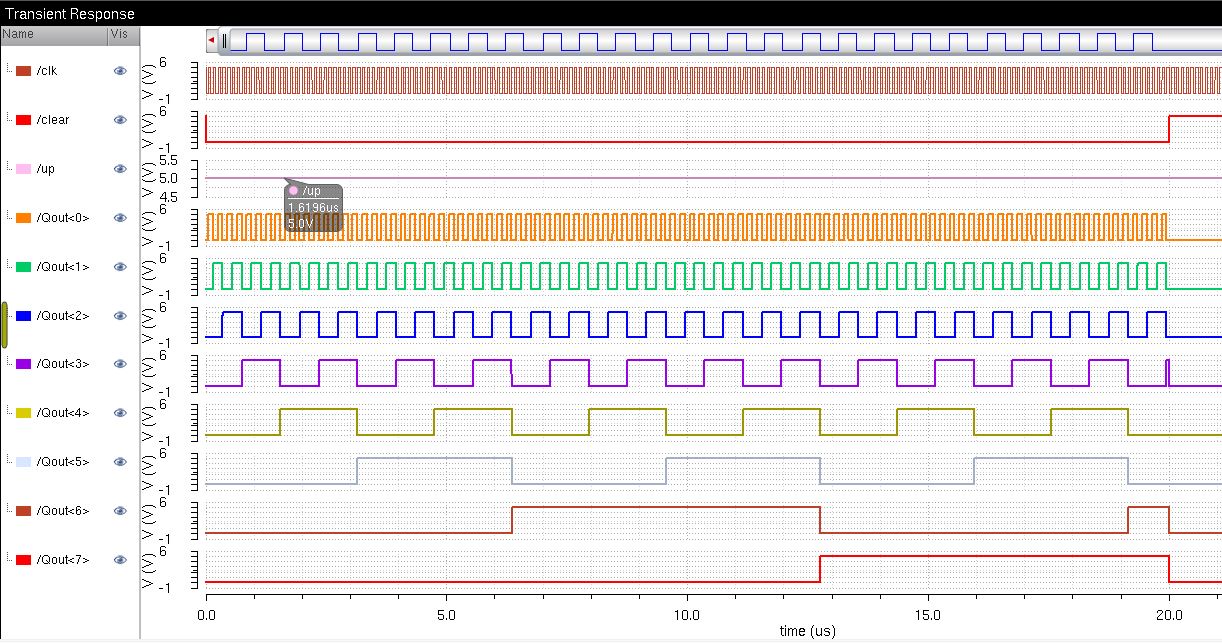
Simulation of all 8 bits counting down, then clearing:
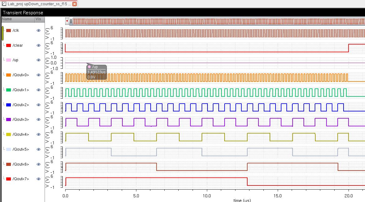
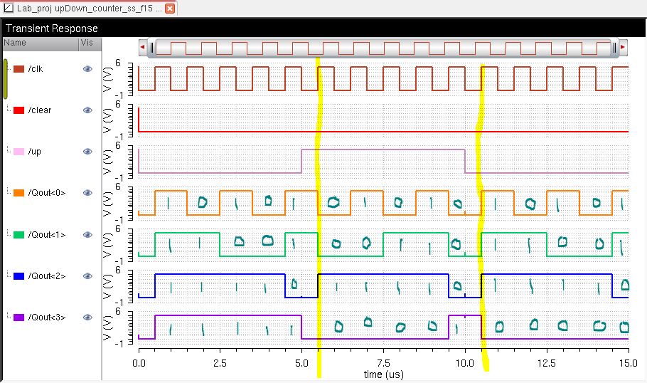
This simulation shows the counter counting up, then down, then up again.
Note: the vertical highlight marks emphasize the rising edge of the clock signal, which is when the register will "load" the new value.
2) 31 Stage ring oscillator:
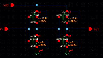
For the ring oscillator, we need to first create a buffer. According to lecture notes on CMOSedu.com, the easiest way to make a good buffer is to use one inverter with both the NMOS and PMOS transistors having a multiplier of 8, then another inverter with multipliers of 64.
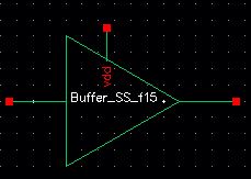
This is done below:
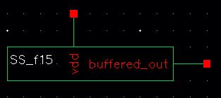
Now we create the schematic and symbol for the 31-stage ring oscillator using buses on the inverter, then buffering the output with the buffer shown above.
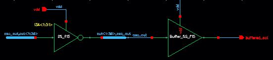
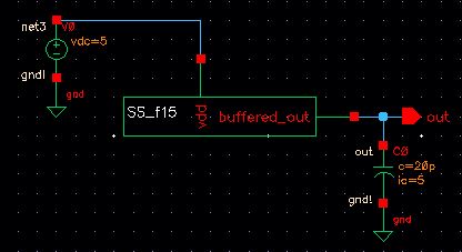
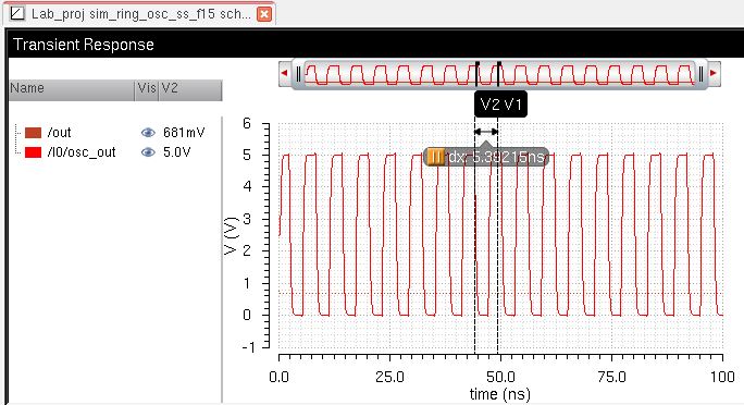
Finally, the oscillator can be simulated driving a 20pF load, as shown below:
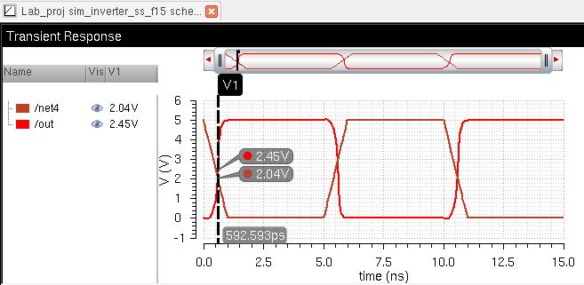
The output is as follows, with a frequency of about 1/5.392ns = 185MHz:
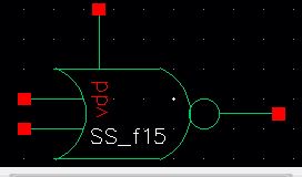
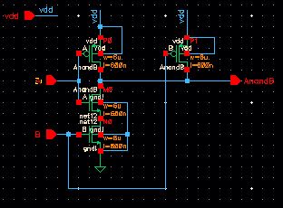
3) NAND gate:
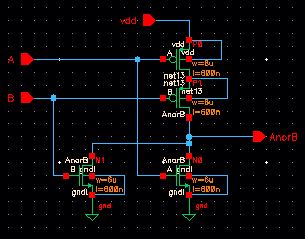
The NAND gate had already been created in a previous lab, but with a global vdd! instead of the vdd pin required here.
The circuit is the same, however:
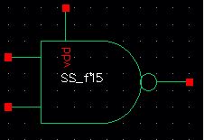
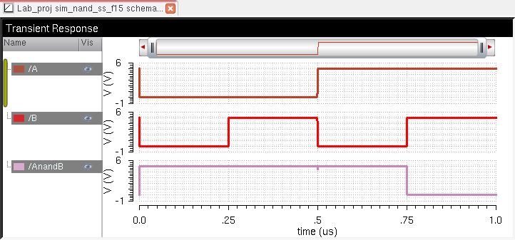
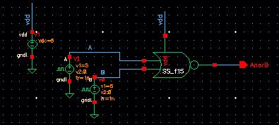
A circuit for simulating the operation of the NAND gate is created:
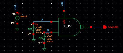
Truth Table for NAND gate: