Lab 8 - ECE 421L
Authored
by Stephanie Silic,
silics@unlv.nevada.edu
November 30th, 2015
Description of lab: This lab report contains the schematics, pin diagram, and testing instructions for chip1.
Project group members:
Jared Hayes
Shada Sharif
Juan Buendia
Stephanie Silic
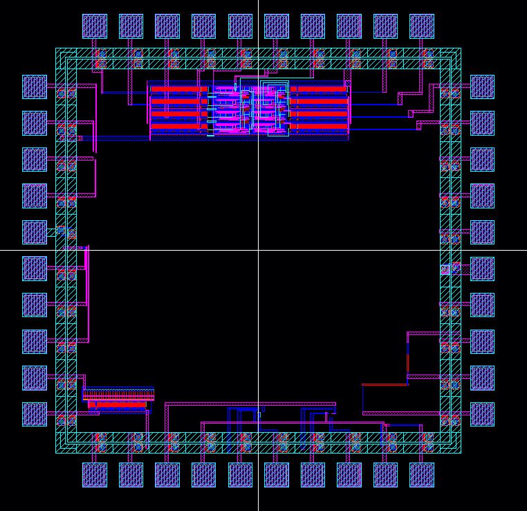
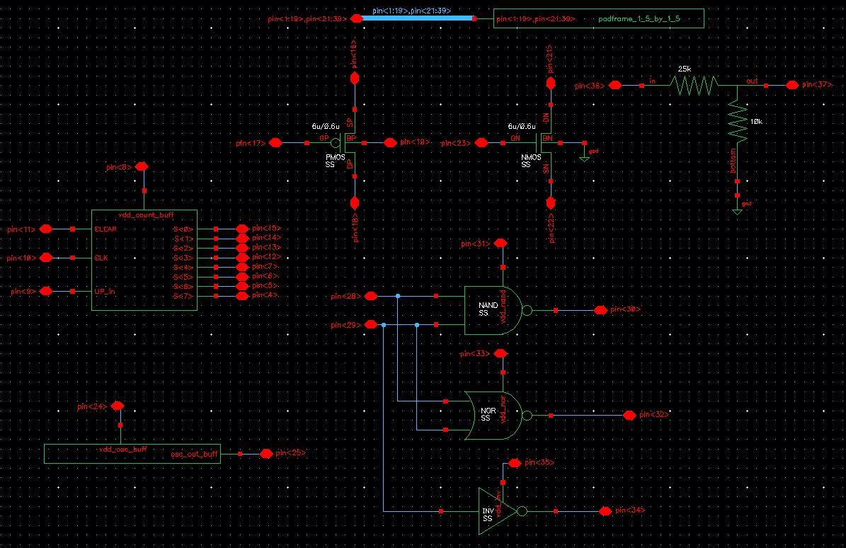
Chip1 includes the following test structures:
- One up/down counter with clear
- A 31-stage ring oscillator with a buffer for driving a 20 pF off-chip load
- NAND gate using 6/0.6 NMOS and PMOS
- NOR gate using 6/0.6 NMOS and PMOS
- An inverter made with a 6/0.6 NMOS and a 12/0.6 PMOS
- Transistors,
both PMOS and NMOS, measuring 6u/0.6u where all 4 terminals of each
device are connected to bond pads (7 pads + common gnd pad)
- Note
that only one pad is need for the common gnd pad. This pad is used to
ground the p-substrate and provide ground to each test circuit
- Voltage divider with a 10k resistor and a 25k resistor
- A 25k resistor implemented using the n-well
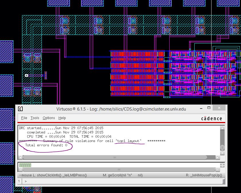
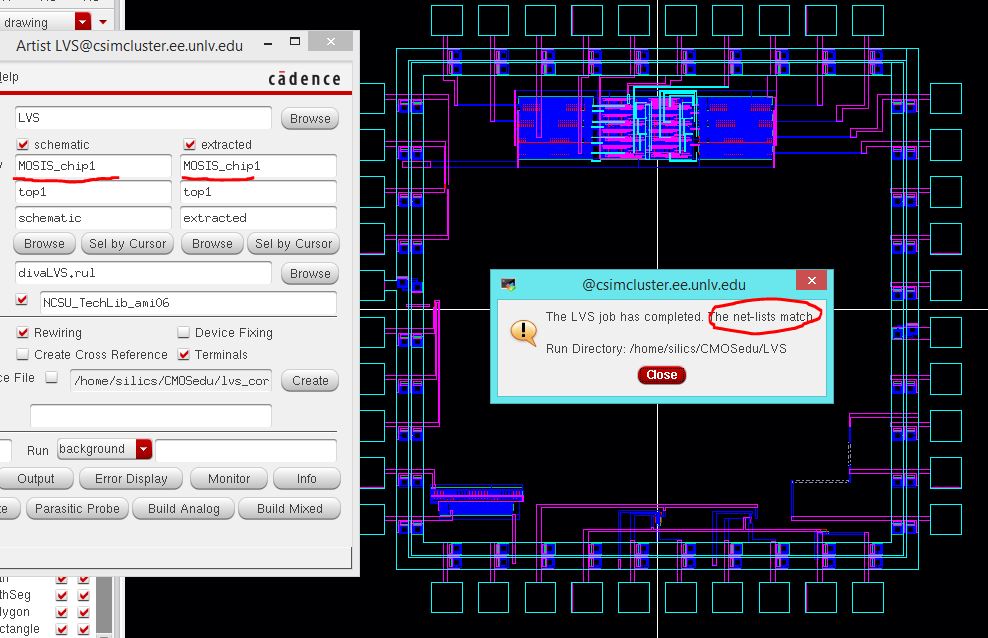
Chip 1 layout:
Here's the schematic:
The chip is on a padframe with pins as shown below:
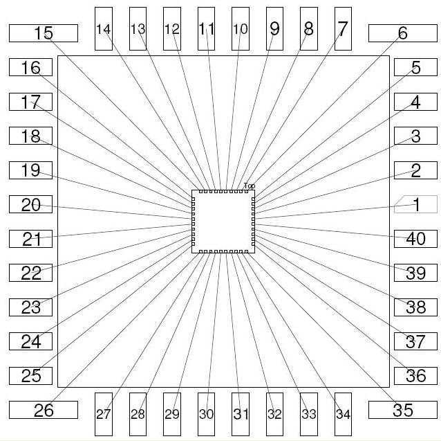
Instructions for testing
A global ground is used, so connect pin<20> to ground to test any or all of the following components:
1) Up/Down counter with clear:
--Connect pin<8> to the vdd for the counter.
--Connect
the UP signal to pin<9>. UP is active high: when UP is
high, the counter counts up, and when UP is low, it counts down.
--Connect the CLK signal to pin<10>.
--Connect CLEAR signal to pin<11>. When CLEAR is high, the outputs are set to 0.
--Connect the 8 outputs as follows, starting with the least significant bit:
-pin<15> --S0 [sum zero]
-pin<14> --S1
-pin<13> --S2
-pin<12> --S3
-pin<7> --S4
-pin<6> --S5
-pin<5> --S6
-pin<4> --S7
2) 31-stage Ring Oscillator with buffered output, capable of driving a 20pF off-chip load.
--Connect oscillator vdd to pin<24>.
--Output of oscillator connected to pin<25>
To test the NAND, NOR, and inverter gates, first connect two input signals, A and B, to pin<28> and pin<29>, respectively. These signals are rounted to the inputs of each logic gate. Then do the following:
3) NAND gate:
--Connect the vdd for the NAND gate to pin<31>
--Measure the output to pin<30>
4) NOR gate:
--Connect the vdd for the NOR gate to pin<33>
--Measure the output from pin<32>
5) Inverter:
--Connect the vdd for the inverter to pin<35>
--Measure the output from pin<34>
6) PMOS transistor:
--Drain: pin<16>
--Gate: pin<17>
--Source: pin<18>
--Body: pin<19>
Connect the body to vdd,
7) NMOS transistor:
--Body: pin<20>
--Drain: pin<21>
--Source: pin<22>
--Gate: pin<23>
8) Voltage divider:
--25k resistor:
First connect pin<20> to ground. Then measure between pin<36> and pin<37>
--10k resistor:
Connect pin<20> to ground, then measure between pin<37> and ground, pin<20>
--Voltage divider:
Connect pin<20> to ground, apply the input voltage to pin<36>, and measure the output between pin<37> and ground, pin<20>
MOSIS_chip1 zipped directory found here for reference.
return to my labs
return to EE 421L page