Lab 7 - ECE 421L 

Authored by Stephanie Silic

silics@unlv.nevada.edu

November 2nd, 2015


Lab Description: This lab details the use of buses and arrays to design multiple-bit word inverters, logic gates, muxes, and includes the schematic, layout, and simulation of an 8-bit full adder.


Lab Report:


Part 1 -- Using buses to create multiple-bit word inverters and other logic gates


First we will draft the schematic for a 4-bit inverter:


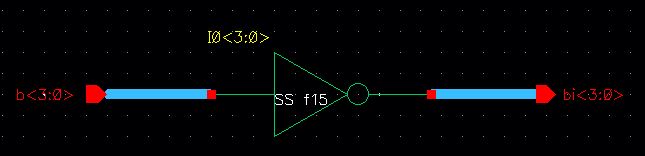
To start off, we use a basic inverter, create the symbol for it, then use buses to make a concise schematic for inverting a 4-bit word. The inverter is given the Instance name I0<3:0> because it will then have 4 inputs and 4 outputs, and the thick wire tool is used to draw the buses, as shown below:


                             http://cmosedu.com/jbaker/courses/ee421L/f15/students/silics/Lab7/4-bit_inv_bus_sch.JPG


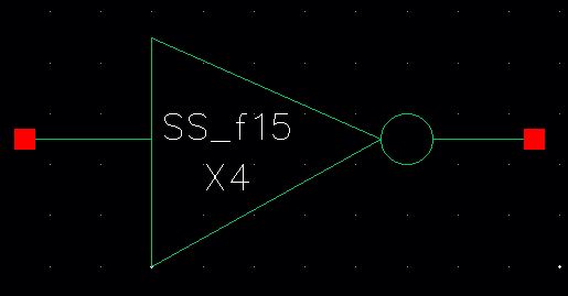
Next we create a symbol that indicates the inverter is a 4-bit inverter:


                                             http://cmosedu.com/jbaker/courses/ee421L/f15/students/silics/Lab7/4-bit_inv_symbol_a.JPG


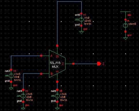
Now we can simulate the operation of this 4-bit inverter, connecting certain outputs to different capacitive loads; this is done using the following circuit:


image


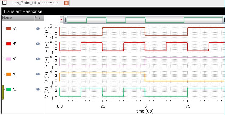
The simulation is as follows:


http://cmosedu.com/jbaker/courses/ee421L/f15/students/silics/Lab7/4-bit_inv_sim_capacitances.JPG


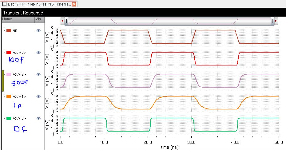
Clearly, the output best displays an inverted output with lower capacitances.


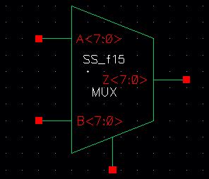
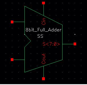
Now, we move on to the 8-bit inverter and logic NAND, NOR, AND, and OR gates:


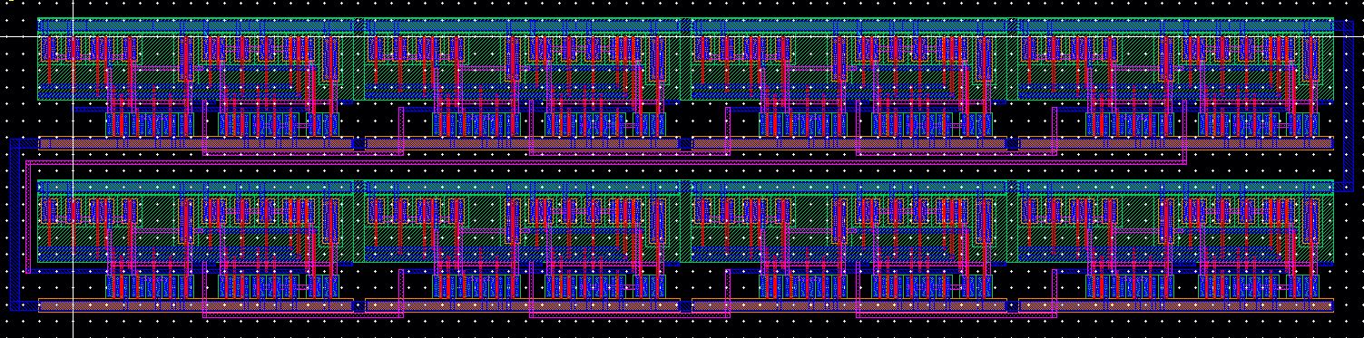
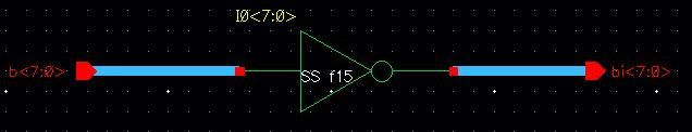
To create the 8-bit inverter, we use the symbol created above and label its name as IO<7:0>. Then we use buses instead of wires so the inverter can take 8 inputs and give 8 outputs . The schematic looks like this:


            http://cmosedu.com/jbaker/courses/ee421L/f15/students/silics/Lab7/8-bit_inv_bus_sch.JPG


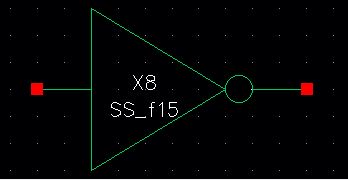
The symbol we will use for the 8-bit inverter:


                              http://cmosedu.com/jbaker/courses/ee421L/f15/students/silics/Lab7/8-bit_inv_symbol.JPG


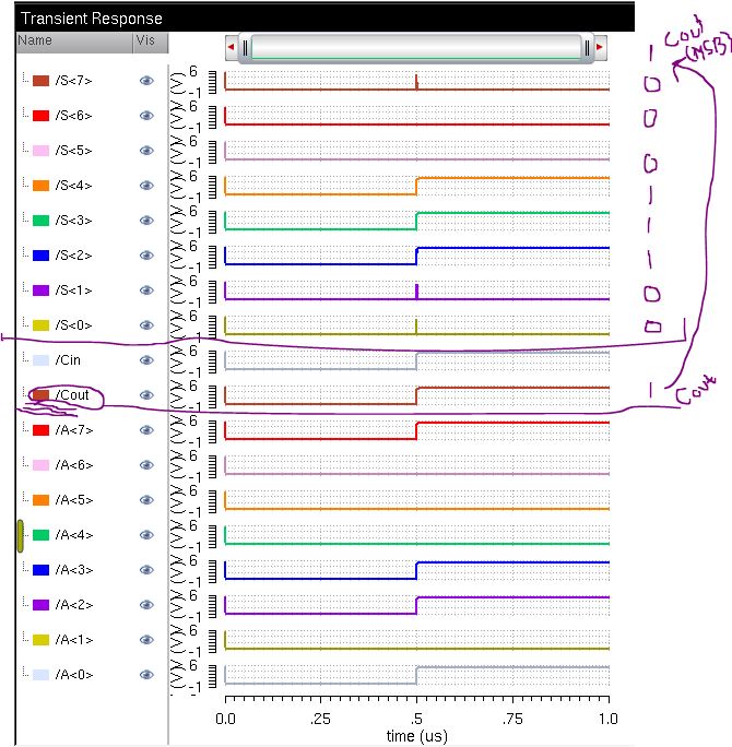
Now, we ensure the 8-bit inverter works by using a circuit with 8 pulse sources going from 0 to 5 V (logic zero to logic one). I have set the 8 inputs to change at .5 us to the following value: 01010101. Thus, the inverted output should be the inverse of that binary word, or 10101010.

The output of the 8-bit inverter with that input is shown below: 


http://cmosedu.com/jbaker/courses/ee421L/f15/students/silics/Lab7/sim_8bit_inv.JPG


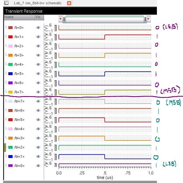
The results are good.


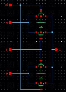
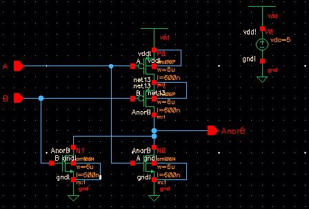
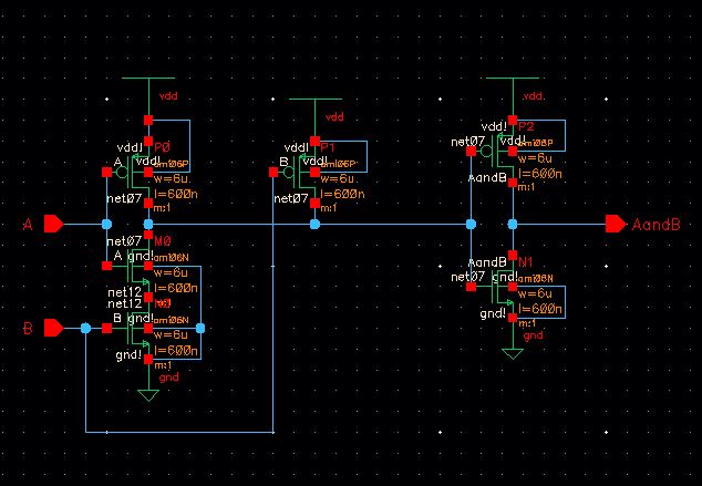
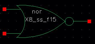
Next, we create 8-bit logic gates. We have already created the NAND and NOR gates in previous labs:

NAND:                                                      NOR:  

http://cmosedu.com/jbaker/courses/ee421L/f15/students/silics/Lab7/nand_ckt.JPG  http://cmosedu.com/jbaker/courses/ee421L/f15/students/silics/Lab7/nor_ckt.JPG


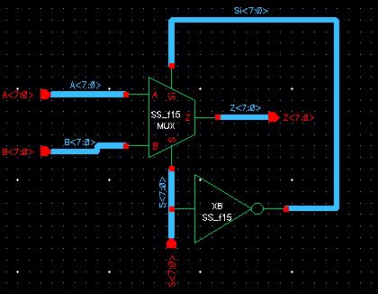
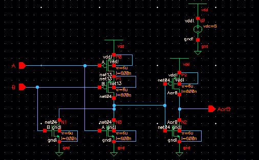
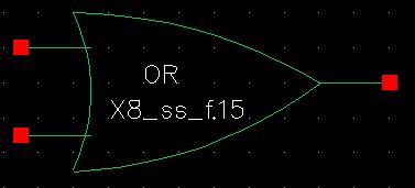
Thus, to create the AND and OR gates, we just add an inverter to the output of the NAND and NOR gates:


AND:                                                                                          OR:


http://cmosedu.com/jbaker/courses/ee421L/f15/students/silics/Lab7/and_ckt.JPG    http://cmosedu.com/jbaker/courses/ee421L/f15/students/silics/Lab7/or_ckt.JPG


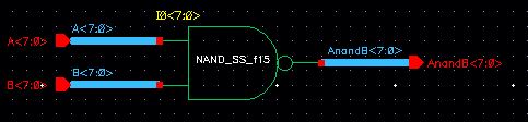
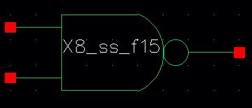
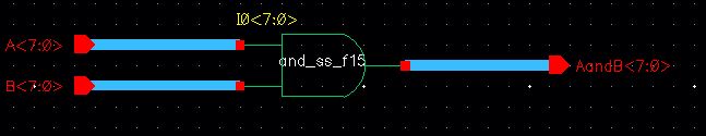
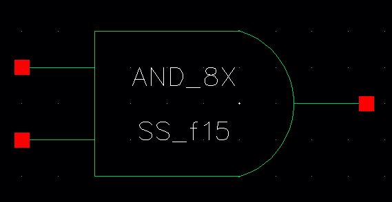
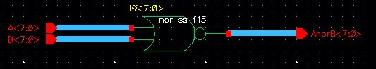
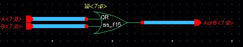
To create the 8-bit logic gates, we use buses as before:


NAND:


http://cmosedu.com/jbaker/courses/ee421L/f15/students/silics/Lab7/8-bit_nand_bus_sch.JPG  http://cmosedu.com/jbaker/courses/ee421L/f15/students/silics/Lab7/8-bit_nand_symbol.JPG


AND:

http://cmosedu.com/jbaker/courses/ee421L/f15/students/silics/Lab7/8-bit_and_bus_sch.JPG http://cmosedu.com/jbaker/courses/ee421L/f15/students/silics/Lab7/8-bit_and_symbol.JPG


NOR:


http://cmosedu.com/jbaker/courses/ee421L/f15/students/silics/Lab7/8-bit_nor_bus_sch.JPG  http://cmosedu.com/jbaker/courses/ee421L/f15/students/silics/Lab7/8-bit_nor_symbol.JPG


OR:


http://cmosedu.com/jbaker/courses/ee421L/f15/students/silics/Lab7/8-bit_or_bus_sch.JPG  http://cmosedu.com/jbaker/courses/ee421L/f15/students/silics/Lab7/8-bit_or_symbol.JPG


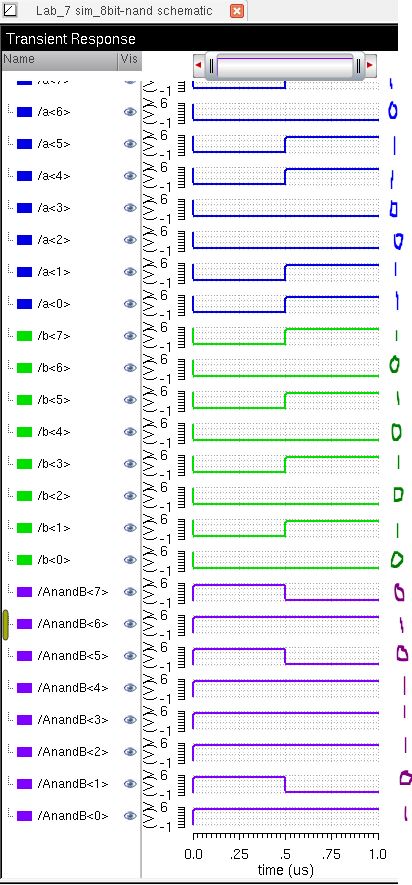
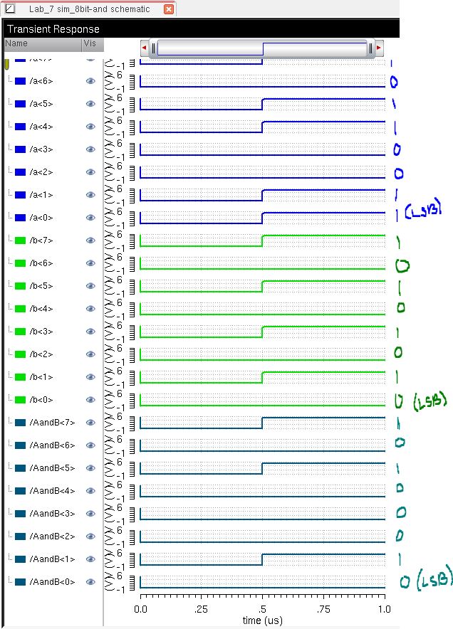
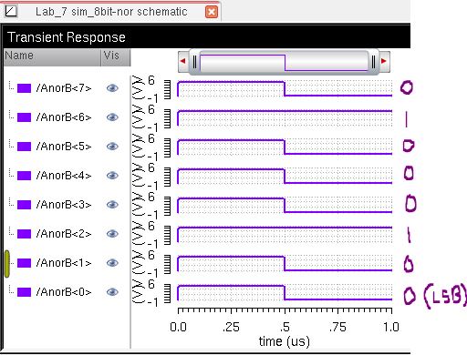
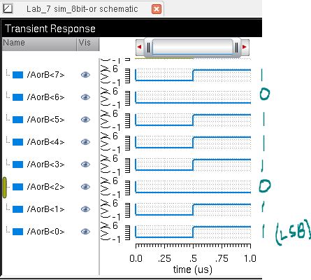
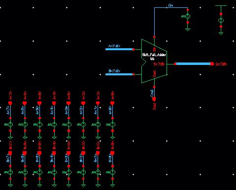
Now we ensure the operation of these 8-bit logic gates by setting up a circuit like the following for each:


                                       http://cmosedu.com/jbaker/courses/ee421L/f15/students/silics/Lab7/schematic-for-simming-gates.JPG


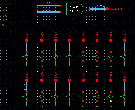
Each of the pulses I need to represent '1' I gave a 1us period, so that at .5 us they will switch to 5V, or logic 1. The inputs that needed to be '0' I gave a period of 4us so that they would not be switching to logic 1 until 2us. Then simulating for 1us will give the results for the two inputs I gave.


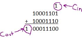
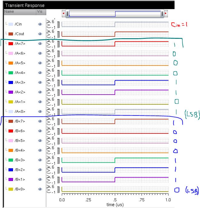
The two 8-bit words I chose will test all four possible cmobinations of inputs to the gates: 00, 01, 10, and 11.  Let A = 10110011 and B = 10101010 (B is the same number used to sim the inverter.)


Since the truth tables for AND, NAND, OR, and NOR are as follows:


ABA and B    A nand BA or BA nor B
000101
010110
100110
111010


 The results from my chosen values for A and B should be as follows (Least Significant Bit on the right):


A: 10110011
B:10101010
A and B:10100010
A nand B:01011101
A or B:10111011
A nor B:01000100
 
The following are the sims for the NAND (left) and AND (right) gates:
 
http://cmosedu.com/jbaker/courses/ee421L/f15/students/silics/Lab7/sim_8bit_nand.JPG  http://cmosedu.com/jbaker/courses/ee421L/f15/students/silics/Lab7/sim_8bit_and.JPG
 
Upon inspection, the results match the truth table.
 
Similarly, with the same input, the output for the NOR (left) and OR (right) gates are as follows:
   
http://cmosedu.com/jbaker/courses/ee421L/f15/students/silics/Lab7/sim_8bit_nor.JPG  http://cmosedu.com/jbaker/courses/ee421L/f15/students/silics/Lab7/sim_8bit_or.JPG
 
These results are what was predicted with the truth table, so this completes the analysis of the logic gates! We can now use 8-bit inverters, NAND, NOR, AND, and OR gates in future projects.
 
Part 2 -- Cirtuit and operation of a DEMUX/MUX:
 
The circuit of a MUX is as follows:
 
                                                                   http://cmosedu.com/jbaker/courses/ee421L/f15/students/silics/Lab7/MUX_circuit.JPG
 
From this circuit, we create a symbol and construct the circuit used to sim the MUX is as follows:
 
                                              http://cmosedu.com/jbaker/courses/ee421L/f15/students/silics/Lab7/sim_MUX_circuit.JPG
 
And finally, using two distinct signals for A and B, and showing the operation when S is high and low, the output of the MUX is this:
 
                     http://cmosedu.com/jbaker/courses/ee421L/f15/students/silics/Lab7/sim_MUX.JPG
 
The operation of a MUX is like a switch. Given a select (S), the output will correspond to either the signal given by A or the signal given by B.
 
Now, we want to create an 8-bit MUX. The schematic will be the following, using an inverter on the Select input so that we only need one select input; the Si input will just be the inverse of S:
 
                                                      http://cmosedu.com/jbaker/courses/ee421L/f15/students/silics/Lab7/8bit_MUX_schematic.JPG
 
And we create a symbol for the 8-bit MUX like this: 
 
                                                                http://cmosedu.com/jbaker/courses/ee421L/f15/students/silics/Lab7/8bit_MUX_symbol.JPG
 
Part 3 -- Full Adder Schematic and layout; 8-bit Full Adder, layout, and simulations:
 
The schematic for the Full Adder is from Fig. 12.20 in the CMOS book. The schematic is as follows:
 
http://cmosedu.com/jbaker/courses/ee421L/f15/students/silics/Lab7/full_adder_sch.JPG
   
From this cellview, we create the symbol for the adder:
 
                                                          http://cmosedu.com/jbaker/courses/ee421L/f15/students/silics/Lab7/full_adder_symbol.JPG
 
And now we use the symbol to create a schematic for an 8-bit Full Adder:
 
                                            http://cmosedu.com/jbaker/courses/ee421L/f15/students/silics/Lab7/8bit-Adder_schematic.JPG
 
The symbol we will use from now on:
 
                                                          http://cmosedu.com/jbaker/courses/ee421L/f15/students/silics/Lab7/8bit-Adder_symbol.JPG
 
Now we must create a schematic to simulate this 8-bit Adder, similar to the one used to simulate the logic gates:
 
                                           http://cmosedu.com/jbaker/courses/ee421L/f15/students/silics/Lab7/8bit-Adder_sim_schematic.JPG
 
To ensure the 8-bit Full Adder is working properly, we can test it by choosing two values to input to the adder that test the Carry in, Carry out, and of course adding.
 
I chose A = 10001101 (decimal 140), B = 10001110 (decimal 142) and Cin = 1.
 
The result of binary addition of these two numbers should be, in decimal: 141 + 142 = 284.
The operation is shown below:
 
http://cmosedu.com/jbaker/courses/ee421L/f15/students/silics/Lab7/Binary_addition.JPG  
 
Simulating the 8-bit Full Adder, I will split up the inputs and outputs for clarity.
 
Inputs:
 
http://cmosedu.com/jbaker/courses/ee421L/f15/students/silics/Lab7/8bit-Adder_sim_inputs.JPG
 
Outputs:
 
http://cmosedu.com/jbaker/courses/ee421L/f15/students/silics/Lab7/8bit-Adder_sim_output.JPG
 
The simulations match the expected values, so the adder is working!
    
Next we lay out the full adder, making sure it DRCs and LVSs:
 
Layout:
 
http://cmosedu.com/jbaker/courses/ee421L/f15/students/silics/Lab7/full_adder_layout.JPG
 
  Full Adder DRC:
 
http://cmosedu.com/jbaker/courses/ee421L/f15/students/silics/Lab7/full_adder_DRC.JPG
 
Full Adder LVS check:
 
http://cmosedu.com/jbaker/courses/ee421L/f15/students/silics/Lab7/full_adder_LVS.JPG
 
Now using the layout for the full adder, the 8-bit Full Adder layout is fairly simple, we just have to rout the Cout bit to the next adder cell, and rout the vdd and ground rails:
 
http://cmosedu.com/jbaker/courses/ee421L/f15/students/silics/Lab7/8bit_Full_Adder_layout.JPG
 
8-bit Full Adder DRC:
 
http://cmosedu.com/jbaker/courses/ee421L/f15/students/silics/Lab7/8-bit_Full_Adder_DRC.JPG
 
8-bit Full Adder LVS:
   
http://cmosedu.com/jbaker/courses/ee421L/f15/students/silics/Lab7/8-bit_Full_Adder_LVS.JPG
 
The last thing we can do is simulate the extracted view of the 8-bit Full Adder, just for fun.
 
http://cmosedu.com/jbaker/courses/ee421L/f15/students/silics/Lab7/8bit-Adder_extracted-sim_output.JPG
 
It is the same!
 
The netlist confirms the simulation used the extracted view:
 
http://cmosedu.com/jbaker/courses/ee421L/f15/students/silics/Lab7/8bit-Adder_extracted-proof.JPG
 
This concludes Lab 7.
 
All work backed up on my PC and email.


Return to EE421L Fall 2015 page


Return to my labs