Lab 6 - ECE 421L
Part 1 -- schematics and layouts of the 2-input NAND gate and 2-input XOR gate
Drafting the schematic of a 2-input NAND gate, with transistors of minimum length and a width of 6um.
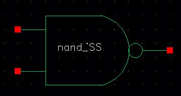
The symbol I will use from now on in circuits for the NAND gate:
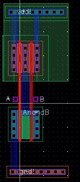
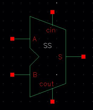
Now, we open a new cell view and begin the layout of the NAND gate, keeping in mind that it should be in a cell frame that is tall, so that we can snap it together with our XOR gate to make the Full Adder:
Now for the XOR gate:
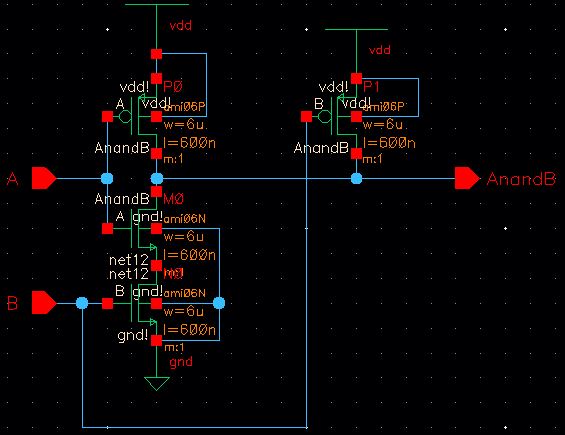
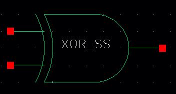
The XOR gate will consist of 6 PMOS transistors and 6 NMOS transistors; the schematic is as shown below, and the symbol:
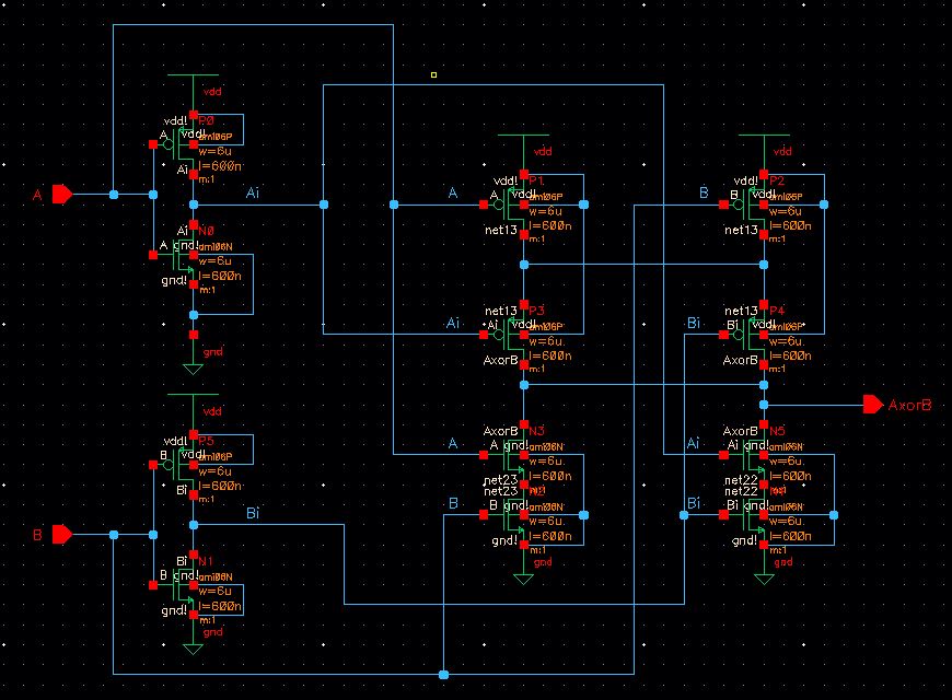
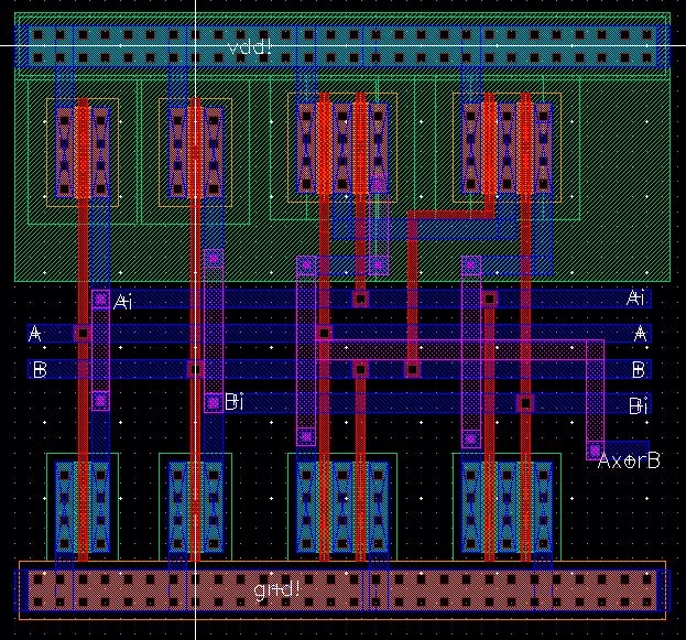
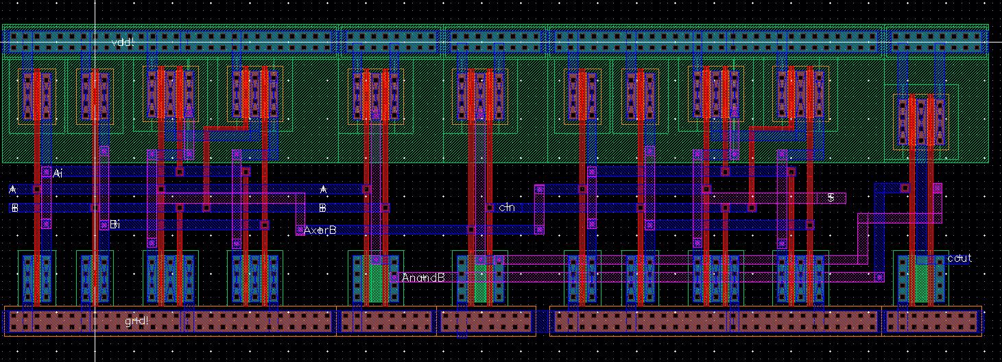
Now, we must create a layout for the XOR gate. With 12 transistors and all those connections, it proves more of a challenge than the simple NAND gate. We must ensure that each connection seen in the circuit above is made using poly1, metal1, or metal2 wires in the layout. After every few connections, I would perform the DRC, and often came up with minor errors: things like the metal wires being too close. The final layout looks like this:
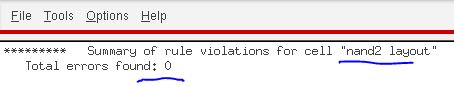
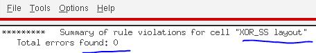
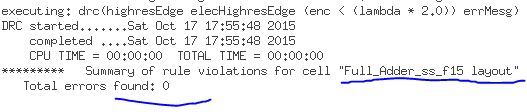
The layout passes the DRC:
In this layout, I made sure A, B, and AxorB could be easily routed to the NAND gate necessary for the FullAdder design. I did not need to have A' and B' routed all the way, however.
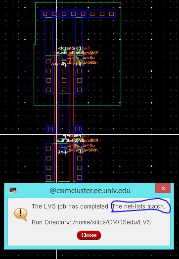
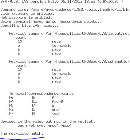
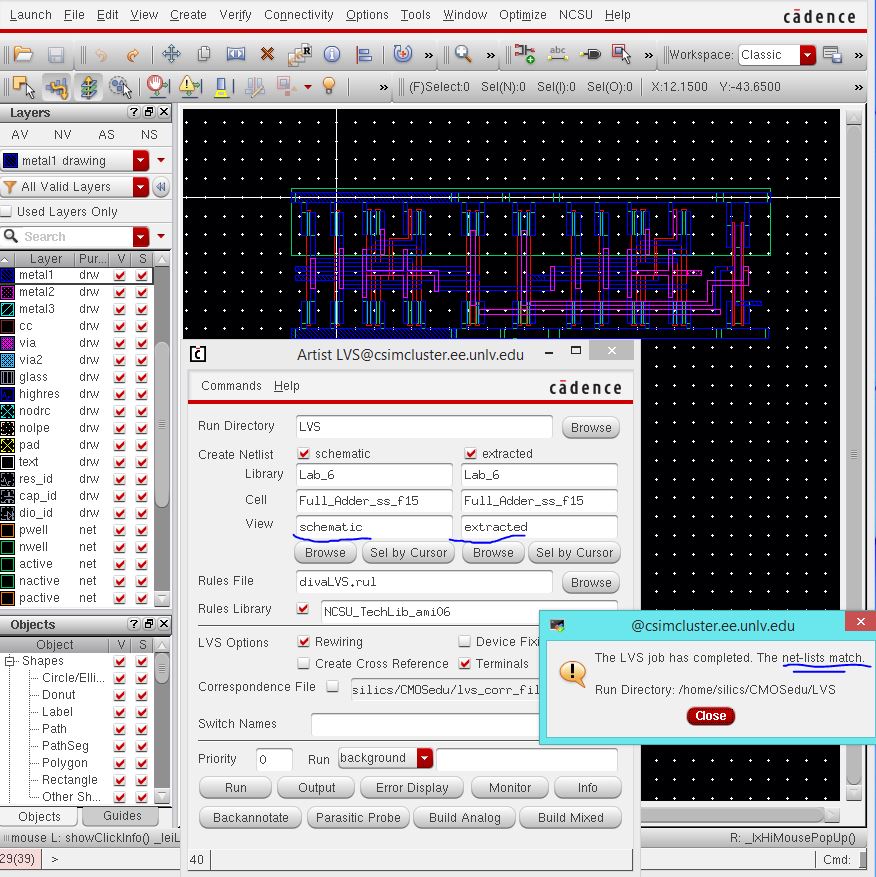
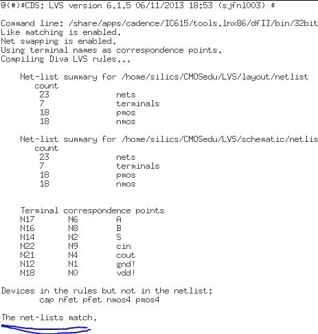
Now, we are ready to perform the Layout versus Schematic (LVS) check. I had two errors in my layout at first; one PMOS transistor was not connected to VDD, and I had failed to connect the AxorB node from between each group of double PMOS and NMOS transistors.
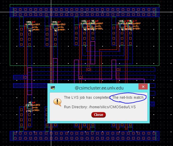
But finally, the LVS was successful:
Part 2 -- Simulation of the NAND and XOR gates
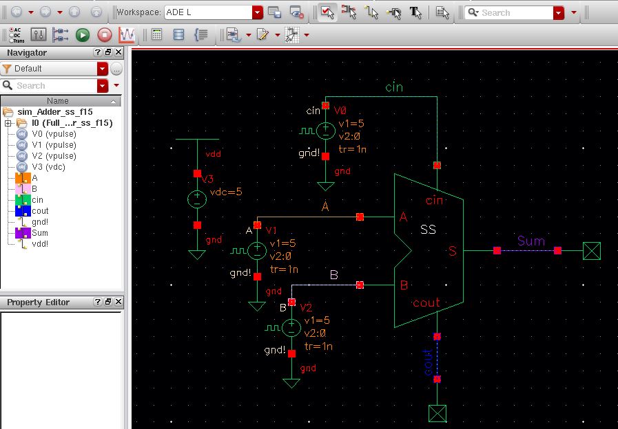
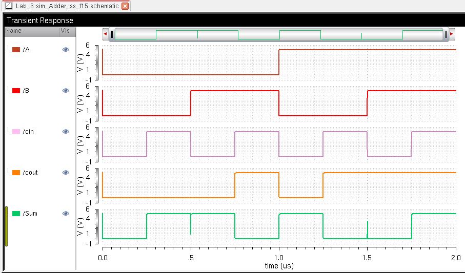
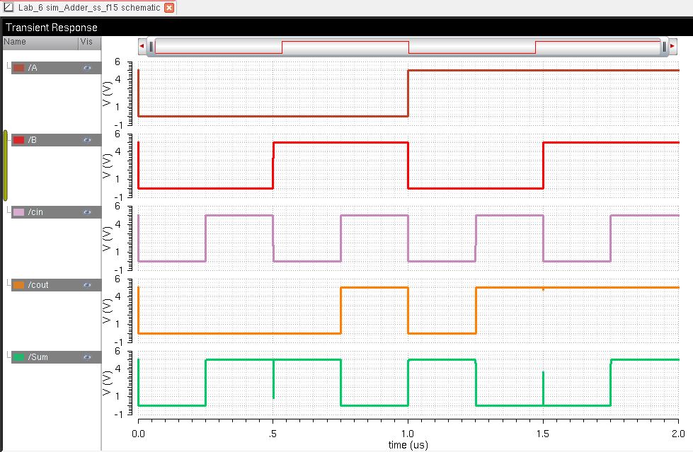
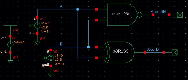
To check the operation of our logic gates, we construct the following circuit:
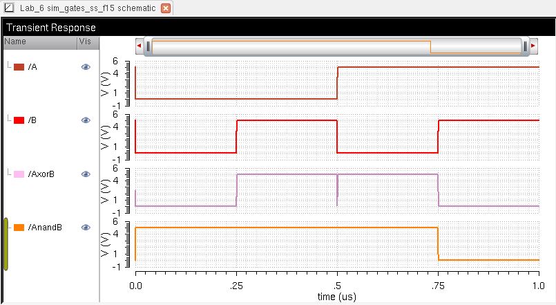
We need to check that the gates follow the values given by this truth table:
| A | B | A nand B | A xor B |
| 0 | 0 | 1 | 0 |
| 0 | 1 | 1 | 1 |
| 1 | 0 | 1 | 1 |
| 1 | 1 | 0 | 0 |
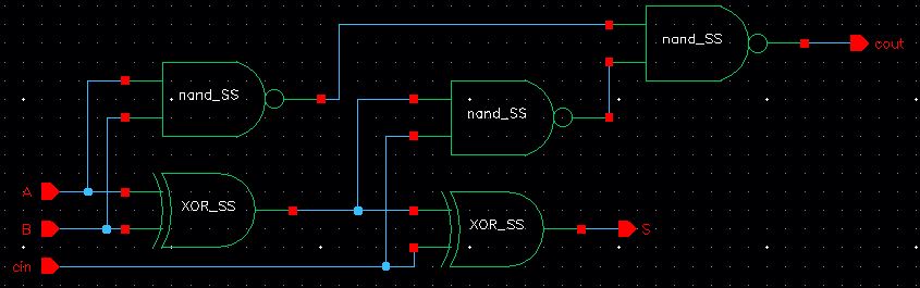
| A | B | cin | S | cout |
| 0 | 0 | 0 | 0 | 0 |
| 0 | 0 | 1 | 1 | 0 |
| 0 | 1 | 0 | 1 | 0 |
| 0 | 1 | 1 | 0 | 1 |
| 1 | 0 | 0 | 1 | 0 |
| 1 | 0 | 1 | 0 | 1 |
| 1 | 1 | 0 | 0 | 1 |
| 1 | 1 | 1 | 1 | 1 |