Lab 5 - ECE 421L
Authored
by Stephanie Silic
silics@unlv.nevada.edu
October 5th, 2015
Lab Description: In this lab we are doing the layout and simulation of an inverter using PMOS and NMOS devices.
We
will be simulating the operation of two inverters, one with a PMOS
length to NMOS length ratio of 12u/6u, and another with a multiplier of
4, so with a PMOS/NMOS length of 48u/24u. Both of these inverters will
each be simulated with capacitive loads of:
-100fF
-1pF
-10pF, and
-100pF
These simulations will be done first with spectre, then with UltraSim. In total, this will give 16 plots.
Lab Report:
Part 1 -- drafting of layouts and schematics:
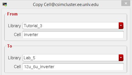
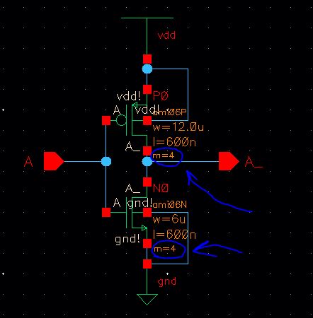
First, we copy in the 12u/6u (PMOS width/NMOS width) inverter from Tutorial 3, created for the prelab.
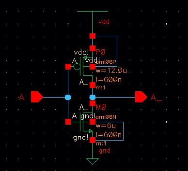
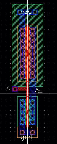
From these cells, we have the 12u/6u inverter schematic and layout (as well as a symbol, which I make use of later):
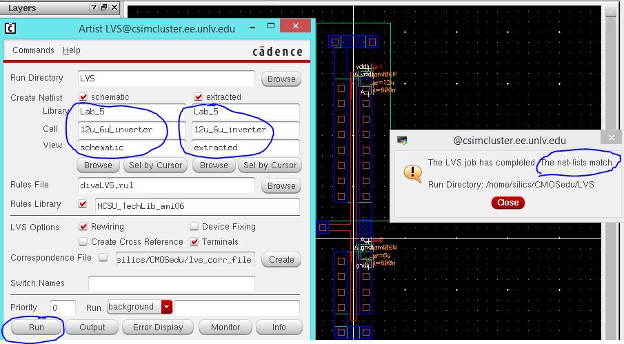
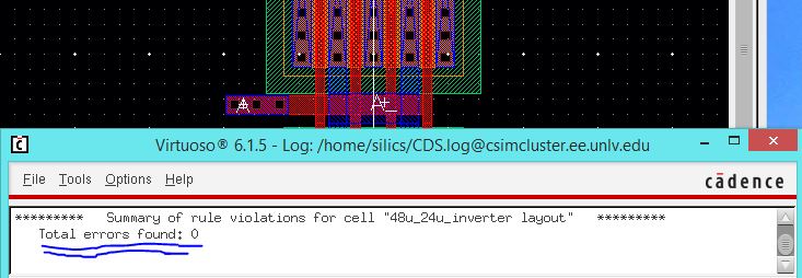
This must all, of course, be checked by doing a DRC and LVS check:
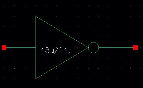
The 48u/24u inverter is drafted in a similar way, but setting the "Multiplier" value to 4.
For
the schematic that will look like this (left): The symbol is
created by clicking Create -> Cellview -> from cellview. (right):
For
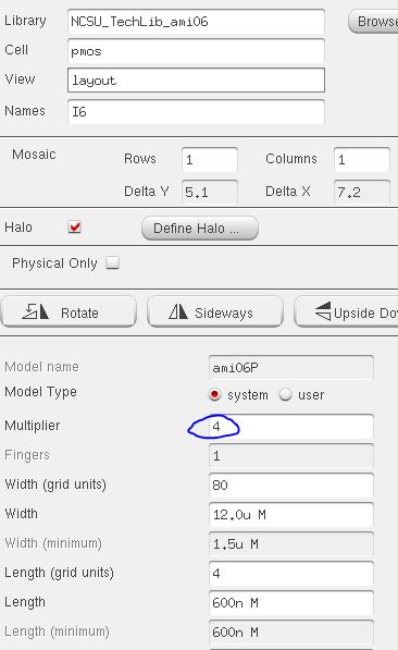
the layout of the 48u/24u inverter we follow a similar procedure:
instantiate a pmos device form the NCSU tech library, and set the width
to 12u, the length to the minimum (.6u) and set the multiplier to 4, as
shown below:
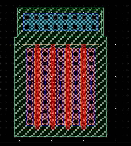
Next, select the ntap from the NCSU tech library, and set the rows and columns of contacts to 2 and 8, respectively:

After
the ntap is placed, the layout looks like the left image below. We
repeat the above process for the NMOS device and ptap, to get the
layout shown on the right:
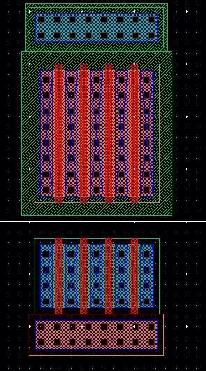
After we connect the metal, add pins (with direction Input/Output!) We get the following complete layout:
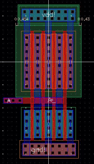
And we ensure that it passes LVS as well:
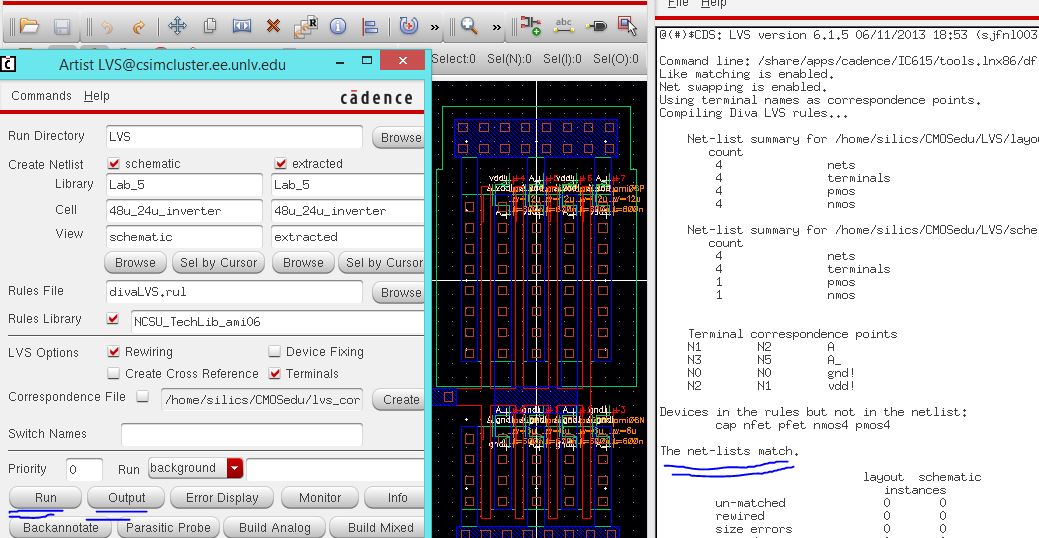
This concludes Part 1: drafting of layouts and schematics, and ensuring they pass DRC and LVS check.
Part 2 -- Simulations
Now, we are ready to start doing simulations. Let's start with the small inverter: 12u/6u.
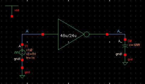
To simulate this inverter, we need to set up a circuit using the inverter with a dc pulse input and a capacitive load:
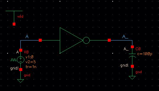
The volage will pulse from 0 to 5, with a 1ns rise time, and a period of 10ns.
Notice
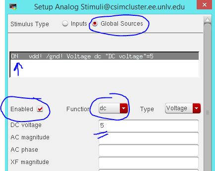
we have to include a Vdd global source in the schematic, because the
PMOS transistor uses Vdd. In my schematic, Vdd is turned on to 5 V dc
using Setup -> Stimuli in the ADE window.
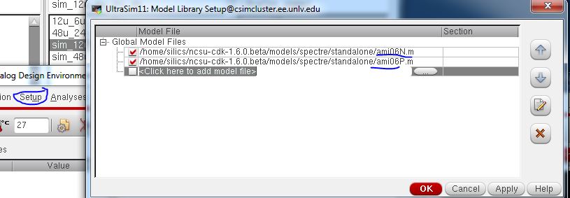
Also, we have to ensure that the model libraries for the NMOS and PMOS devices are included:
Now we set up the simulation parameters, doing a transient simulation for 25ns, or 2 and a half periods.
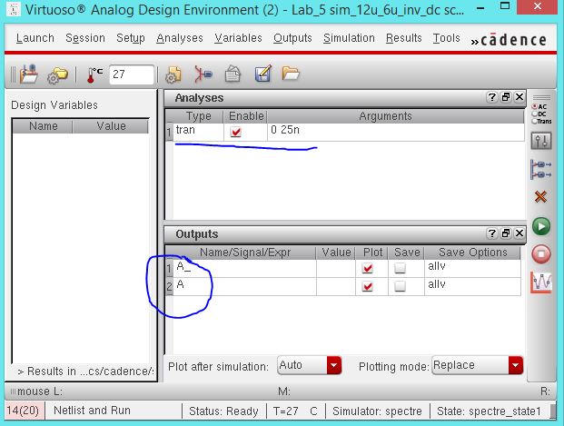
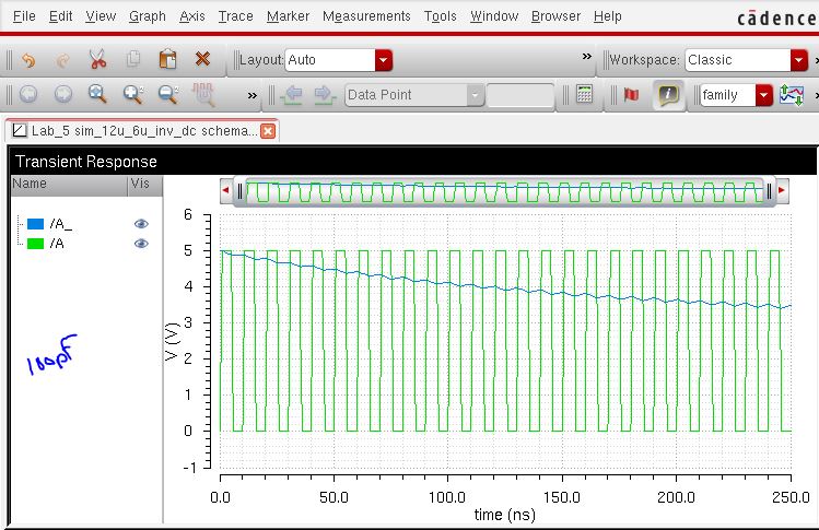
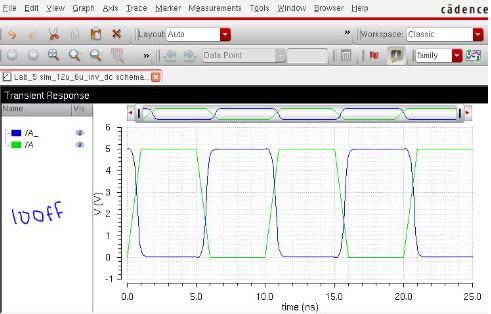
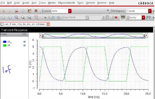
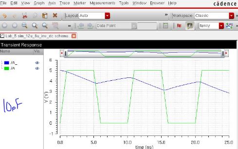
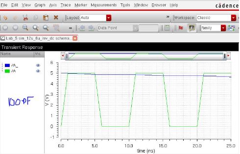
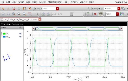
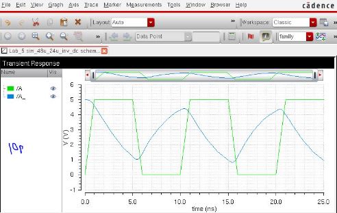
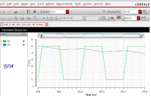
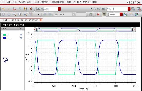
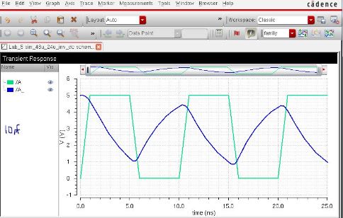
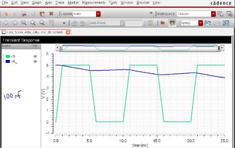
Finally, using spectre, the 4 following simulation results are in order of increasing capacitive loads: 100f, 1p, 10p, and 100p
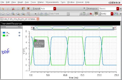
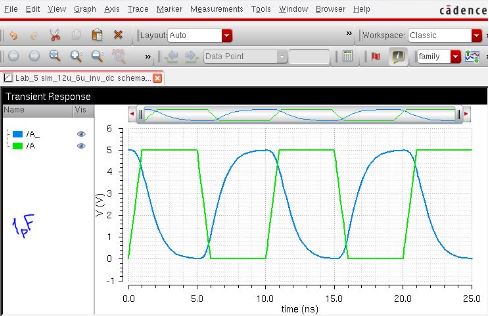
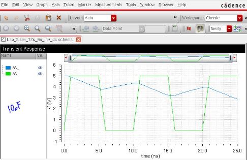
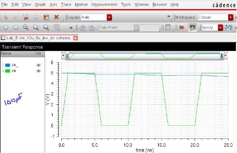
As we can see, as the capacitive load gets larger, we begin to lose the inverting atributes of the inverter.
In
fact, any larger than 1pF will not provide a good inverted output.
Instead, what happens is that the output slowly drops in value as the
capacitor gets discharged, and the output looks like a triangle wave.
The following sim illustrates this by showing the 100pF load sim done
for 30 periods, instead of just 3:
Now,
the simulations are repeated using UltraSim. We change to UltraSim by
clicking on Setup -> Simulator/Directory/Host and clicking on
UltraSim from the dropdown box:
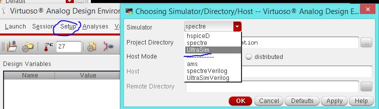
Note: The
NMOS and PMOS model libraries will have to be re-included. Finally, we
get the the following 4 schematics, which are identical to the ones
done previously, only now I am using UltraSim:
The simulations give the same results!
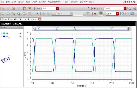
For the bigger inverter (48u/24u), we draft a similar schematic for simulating:
Once
again, we must set the global source, vdd, to 5 V in the Setup ->
Stimuli window, ensure we have the NMOS and PMOS model libraries
referenced.
The following four simulations are done using spectre, in order of increasing capacitance:
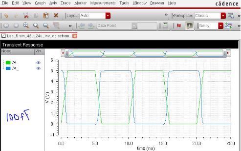
Once more, the simulations indicate what we learned from the small inverter: that as capacitance increases, the performance of the inverter gets worse.
This time, however, the results seem slightly better, with the 1pF load
giving fairly good results, and only getting substantially worse around
10pF.
Finally, we change the simulator to UltraSim, re-include the NMOS and PMOS libraries, and do the four simulations again:
This concludes part 2.
All work backed up in Google Drive:
Return to EE421L Fall 2015 page
Return to my labs