Lab 6 - EE 421L
Authored
by Emmanuel Sanchez,
Email: sanch512@unlv.nevada.edu
10/05/2015
Lab
description:
Design, layout, and simulation of a CMOS NAND gate, XOR gate, and Full-Adder
Pre-lab work
- Back-up all of your work from the lab and the course.
- Go through Cadence Tutorial 4 seen here.
- Read through the lab in its entirety before starting to work on it
- Draft
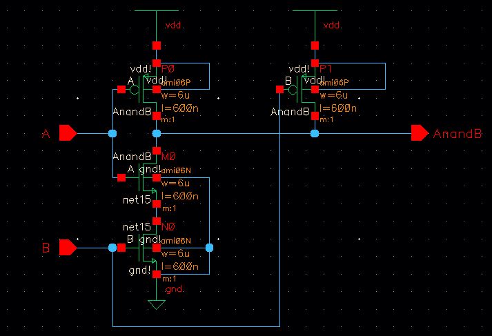
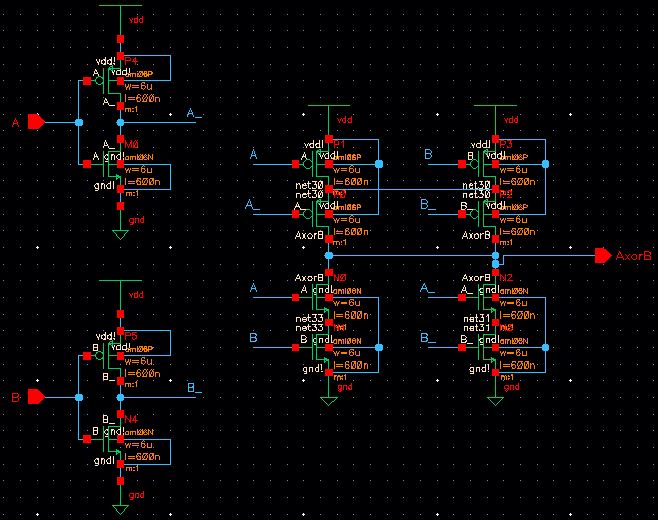
the schematics of a 2-input NAND gate (Fig. 12.1), and a 2-input XOR
gate (Fig. 12.18) using 6u/0.6u MOSFETs (both NMOS and PMOS)
- Create layout and symbol views for these gates showing that the cells DRC and LVS without errors
- ensure
that your symbol views are the commonly used symbols (not boxes!) for
these gates with your initials in the middle of the symbol
- ensure all layouts in this lab use standard cell frames that snap together end-to-end for routing vdd! and gnd!
- use a standard cell height taller than you need for these gates so that it can be used for more complicated layouts in the future
- ensure gate inputs, outputs, vdd!, and gnd! are all routed on metal1
- Use cell names that include your initials and the current year/semester, e.g. NAND_jb_f19 (if it were fall 2019)
- Using Spectre simulate the logical operation of the gates for all 4 possible inputs (00, 01, 10, and 11)
- comment on how timing of the input pulses can cause glitches in the output of a gate
- Your html lab report should detail each of these efforts
- Below
shows (click for a larger image): 1) schematic of a 2-input NAND gate,
2) schematic of a 2-input XOR gate, 3) simulation schematic, 4) example
pulse statement to generate a digital input, and 5) simulating the
operation of the gates for all 4 possible inputs.
Lab Report:
Schematics for 2-input NAND gate and 2-input XOR gate (both using MOSFETS of size 6u/0.6u).
Symbol views of NAND and XOR gates.
Standard cell layouts and DRC of NAND and XOR gates:
- The standard cells allow us to easily route vdd! and gnd! by snapping the cells side by side.
LVS of NAND and XOR gates:
Schematic used for simulation of all gates (inverter, NAND, XOR).
 | 
Pulse settings for A input. | 
Pulse settings for B input. |
Simulation of schematic and extracted of inverter, NAND, and XOR gates:
 
Schematic Simulation
| 
Extracted Simulation
|
Schematic and symbol for Full Adder:
Full Adder layout and DRC:

Full Adder LVS:

Full Adder schematic for simulation:

Full Adder simulation (schematic and extracted):
Full Adder truth table:
 | Simulation of schematic:

|
Full Adder truth table
| Simulation of extracted:
 |
Notice
there are a few glitches occuring at the output of the Sum and Cout.
These glitches are caused because of the rising and falling delays in
the input pulses. For example, if we have two different input
combinations that generate the same Sum and we input them one
immediately after the other, the small time during which the inputs
transition cause a glitch in the Sum because the voltage levels are not
steady for that brief moment. If the input pulses were ideal, the
glitches would not occur.
Here is a link to download my lab6 library and files:
lab6.zip
Return to EE421L Labs