Lab 7 - ECE 421L
Authored
by Mari Gilligan
Email:mgill19@unlv.nevada.edu
11/01/2015
Prelab7:in this prelab we are going through "Tutorial_5"
This
Tutorial is about design and layout of operation of ring oscillator.the
main focuse is on how to use arrays and buses in this lab.
so lets begin by coping the Tutorial_4 library into Tutorial_5 library,dont forget to update insttances as well.
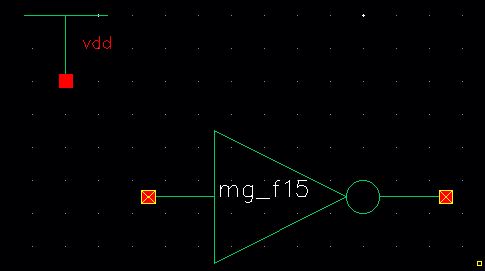
create
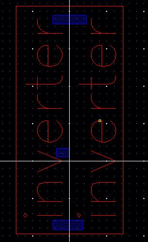
the new schematic cell view and call it ring_osc.and place the cell
view of the invereter that was created in Tutorial_3.also place vdd!
symbol from supply net.
Like this :
Next
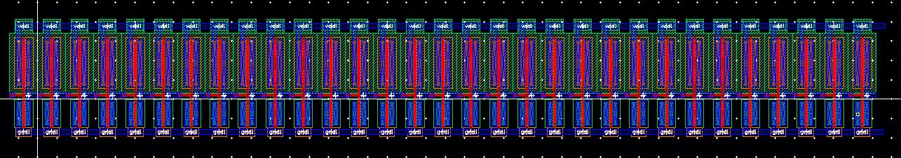
press C for( copy) and the inveretr (to copy the inverter).before
placeing the copy of the inverter press F3 and make the colums to be 30.
This creates 30 ring inverter that we can place them together insted of doing the process 30 times.(especial option).
Then
instanciate the first copy of the inverter on the output of the
existing inverter .reapeat for the second copied and we should have
this:

Now
add a wire connection the output of the last invereter to the input of
the first inverter.,Lable your wire as osc_out ,
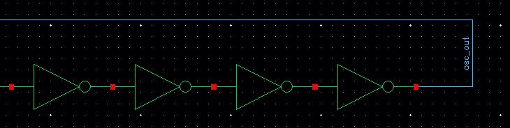
then check and save your schematic.
start
the ADE_L,and set up the simulation process and at this point everyone
should know how to get the model libraries and so on...
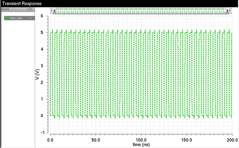
run the tran simulation for 200ns and we should het this:
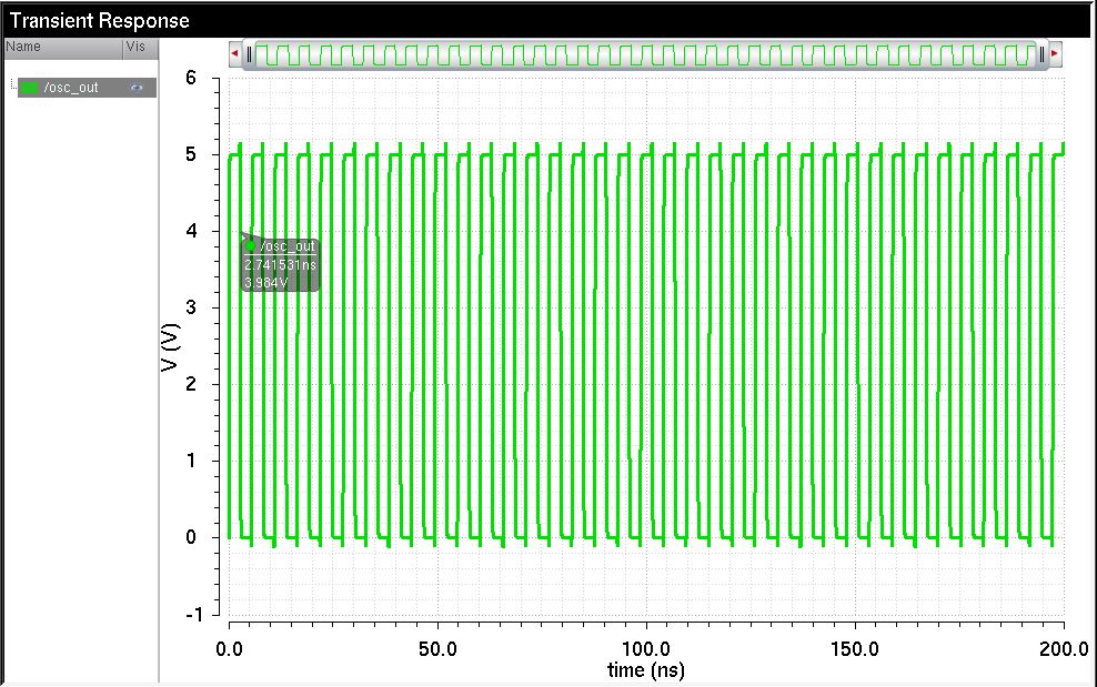
In the real circuit we would have a noise ,lets take care it by going to have the initial condition.
so
go to -> simulation and click on the Convergence aids->initali
condition.select the node voltage of 0 and click on the wire
labled osc_out.then press ok and run your simulation again:
and we will ahve the same results .save your state and close the ADE.
Now Lets make the schematic more Pleasent to look at:
Plave
the inverter and chnage the anme of that by ->press Q,and make it
I0<1:31> and press ok,I hope we understand this is equal to
placing 30 inverter together.I use thw Wire and made them thick(0.04 )
for thickness of the wires and places them as you see here.
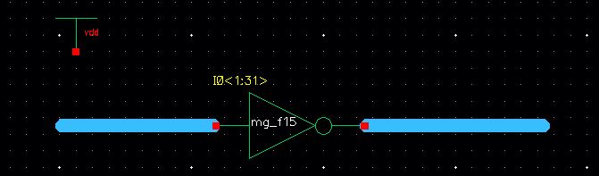
Lable your wires and check and save your schematic.
lets go ahead and make our Layout for our invereter.
create
a layout cell view for the ring oscillator and place the two inverters
layout in the cell next to each other .DRC your layout so you dont have
any erros.
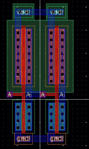
add
a rectangule of metal1 between the vdd! ,Ai of the first inverter and A
of the second inverter.and gnd! as you can see here .the display is set
to 0 to see where the metal1 connection is located.
set
your display mode back to 10 and delete the right inverter.nect select
of the inverter and press C for copy,again we can use F3 and put the
number of colums to 30.press ok and plce them back to back next to each
other ,do the process very carefully ,so you dont have DRC erros.
Like this:
add via (m2-m1) to the left and right of the firat and the last inverter.
Next
add metal2 to connect this vias from fist inverter to the last one ,set
the display mode to 0 so you can see better whats going on.
Next add
pins for gnd! and vdd both have the direction of input output,and
osc_out has a output direction..the vdd and gnd on metal 1 oand the
osc_out on metal2.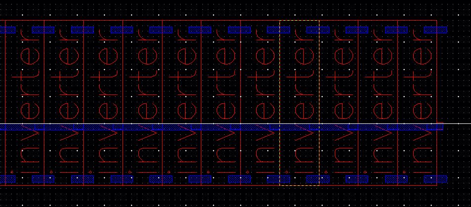
DRC your layout and make sure that you dont have any erros.
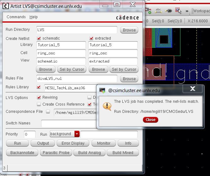
extract the layout and run LVS,
the
LVS is failed due to the different in output pin for osc_out ,so lets
add that to our schematic and check and save ,also notice that the wire
connections has to be labled as well.
run the LVS again you should get this results:
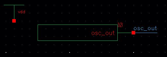
now delete the vdd! symbol from your schematic and create the symbol, for the ring oscillator.
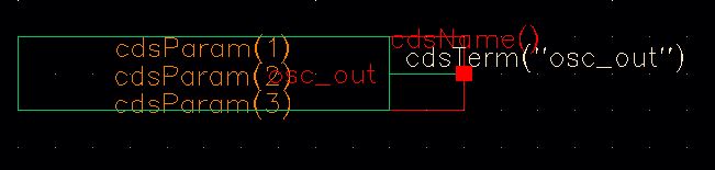
cretae
the new schematic cell view and call that sim ring_osc and place the
ring _osc and vdd symbol in this cell.Then add a wire to the output of
the ring osc symbol and lable that as osc_out.
check and save your schematic.if you get errors for foating net/wire go to ->check->find marker-> press ignore.
Luanch the ADE and enter the models ,stimuli,output to plot ,and all the setups like we usually do.....
dont forget to set the initial condition as well and save the state and run your simulation.
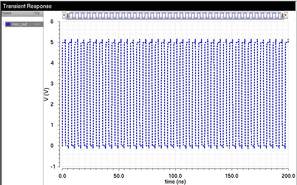
lets
simulate the extracted view as well,as before use setup->environment
to enter the extracted before schematic .press ok and we should have
this:
save
and close everything ,dont forget to change the changes we made to
simulate the extracted view,we should go back and remove the extracted
,so we dont simulate extracted insted of schematic for later simulation processes.
End of Prelab 7
Post lab7 :
First Read through the entire lab before starting it .
Now :
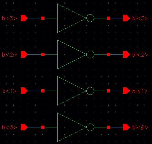
Lets
start by 4_bit inverter which i use the 4 inverters that we made in
tutorial_5.then creating 4 inputs and outputs and call them bi
and b,as here:
4_bit inverter:
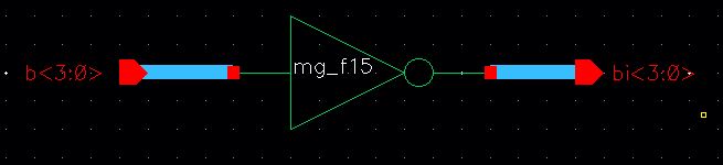
then
make a equivalent schematic which is much easier and much more compact
from the previous one.this process starts by instanciate the inverter
and add the thick wire which we call it input b<3:0> which shows the
4bit and b<3:0> for output .Please dont forget to chnge the inverter to
4_bit by going to ->click on the symbol of the inverter
and press Q,then you are able to change the instance name to
I0<3:0> and push the value bottom to be on ,. for a 4_bit
inverter.
compact design of 4_bit inverter:
now make a symbol from this schemtic which is for 4bit inverter,.like we did earlier.
Simulation of 4_bit inverter:
Now
we are going to use the symbol that we just created for our 4_bit
inverter to do simulation.if you recall, in the prelab we
were required to use capacitor and see the
effect of the capacitors on the inverter ,so lets do that:
I
set up 3 caps with the values of 1p,500f,100f, also note that im going
to have a pulse for my input with 5ns and a 10ns period,.
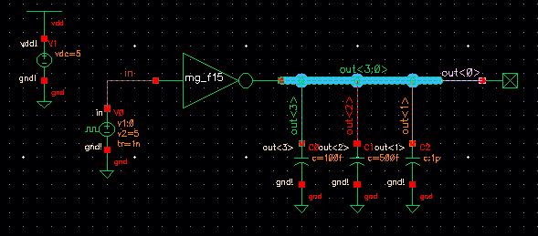
Luanch ADE_L and run the transient for 50 ns ,.
we notice that the incresing in the capacitance reduces the rectangular shape of the input into more curved wave.
Next:
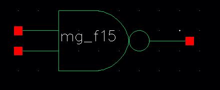
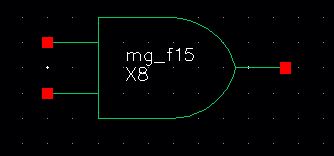
8_bit NAND gate schematic:
we need to make a 8_bit nand gate ,so i made my schemtic and my symbol like here:
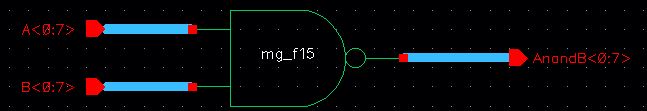
Symbol:
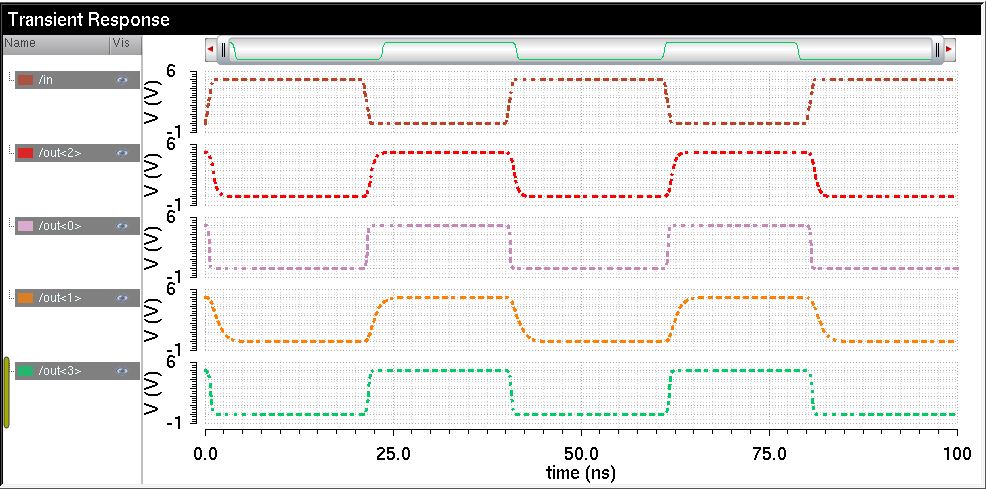
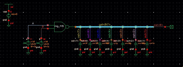
8_bit NAND gate simulation:
Like
before we need to show our circuit works properly,so simulate the 8_bit
nand gate ,and we will see how the higher capacitance has effect
on the shape of our squre wave.
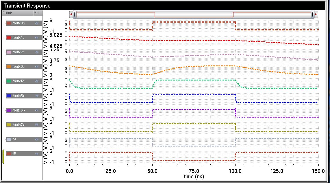
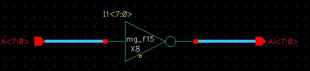
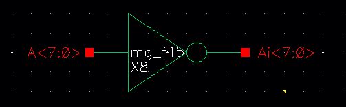
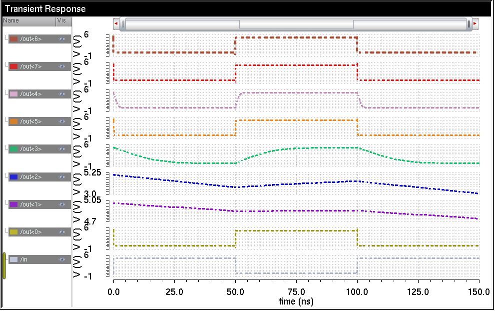
8_bit Inverter:
we
can reapeat the process that we did earlier to make 4_bit inverter, and
just implemente the 8_bit which is <7:0> for our inverter symbol.
8_bit inverter simulation:

NOR gate :
i will start my NOR gate by 1-bit first,then i can easily implement it for a 8_bit NOR gate.
NOR schematic
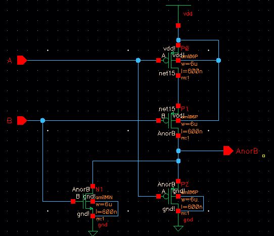
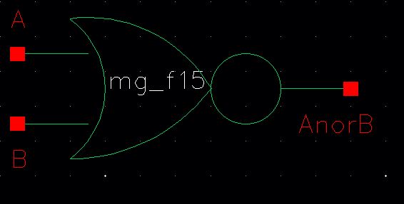
NOR symbol:
8_bit NOR gate schematic:
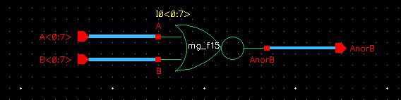
symbol of 8_bit NOR gate:
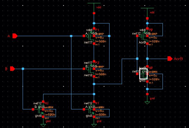
OR gate schematic:
since we created NOR gate above ,its easy to get OR gate from the same schemtic by adding an inverter.
OR gate symbol:
repeat the process for the 8_bit OR gate .
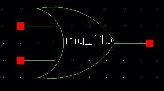
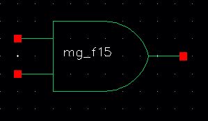
AND gate schematic:
the same process as before ,take the nand schematic and add an inverter :
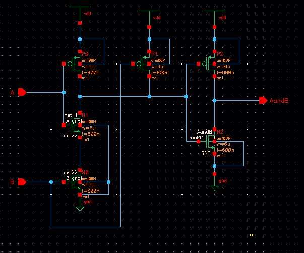
AND gate Symbol:
B_bit AND schemtic:
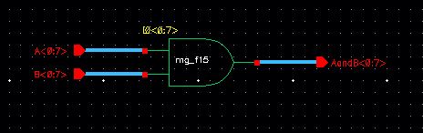
8_Bit AND gate symbol:
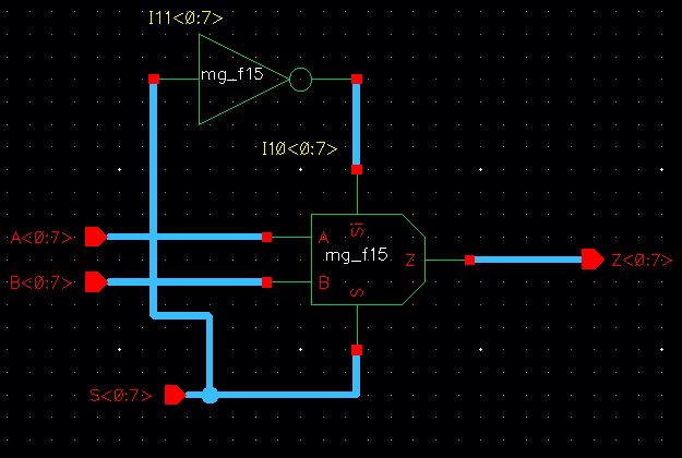
2_1 mux Schematic:
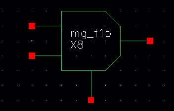
2_1 Mux Symbol:
we
need to simulate our mux ,layout the schematic and add input to the
circuit,notice we will have two inputs which one is going to be twice
of the speed of the another one.be ensure that S and SI are opposite of
each other,one of my voltages goes from 0-5v and the other one goes
from 5-0.this gives us S and Si opposite of each other.
Mux simulation:

we
notice that in the simulation ,when S is 1 and si is 0,the output is A,and
the output is B.the mux goes back and force between A and B,
depends on S.
DEMUX design:
Now
the demux is opossite of the mux in terms of input and output,.they
change around,S would be a slecet if the signal from Z goes to A or B..
we
should have a 8_bit Mux Now,so im going to make a schematic as follow:if
we use the inverter we wont need to have the S and Si input pins.
8_bit mux schematic:
8_bit Mux symbol:
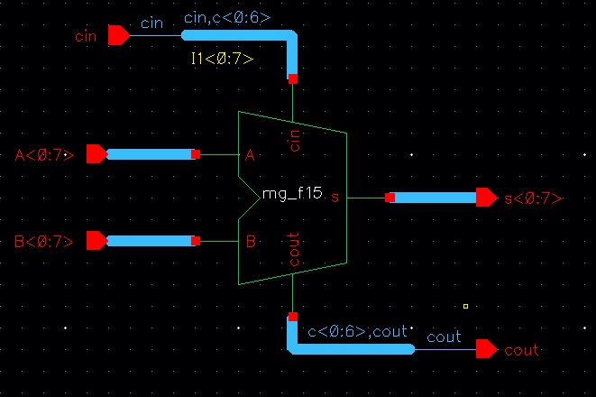
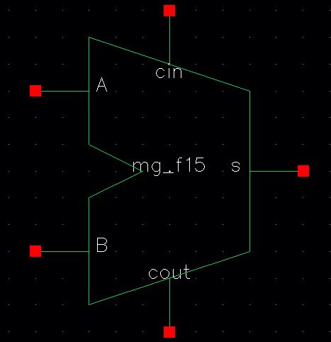
Full adder:
for
the design of the full adder since it different from what we had in the
previous labs,im going to use the NMOS, PMOS of W=6u.
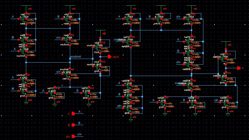
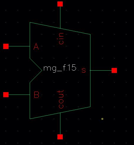
Symbol:
8-bit adder Layout :
i will layout 1 bit adder first then it make it easy to make 8_bit adder and being able to keep track of the connections.
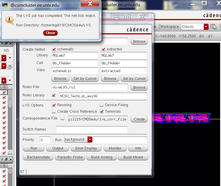
DRC and LVS your layout and make sure that there isnt any erros.
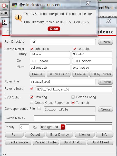
8_bit adder schematic:
8_bit adder symbol:
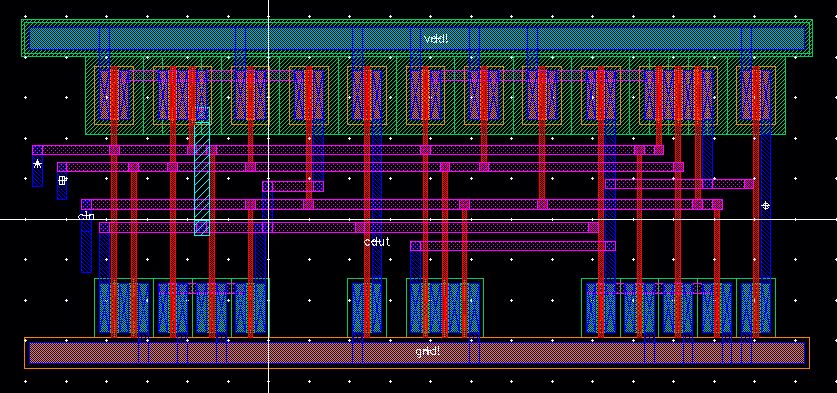
creat the layout of 8_bit adder :
when we made sure there is no error,we can use our 1-bit layout and make the 8_bit layout from it,.
get
the 1-bit adder and instanciate that to the new layout that you call it
8-bit adder.click of the enire layout and press C for copy and place
them next to eath other and connect the carry to the next one.Then add
(cin ,cout) and the other input output pins.remember to add A ,B and S
pins as a part of an array.like this:
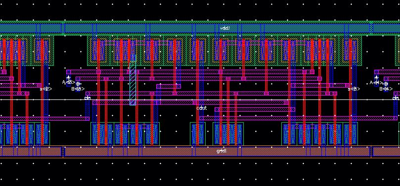
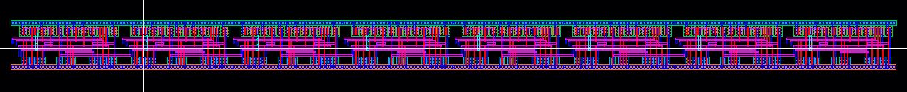
DRC and LVs your layout for ensuring that there arent any errors.
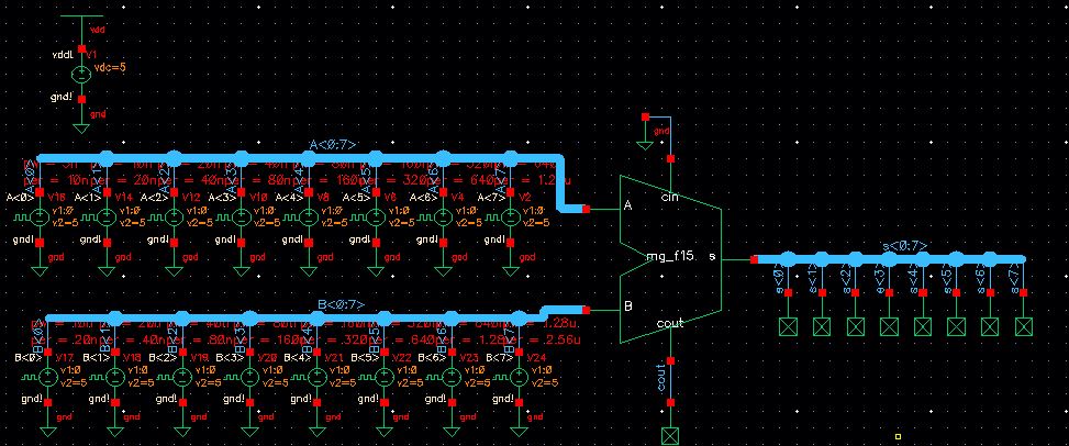
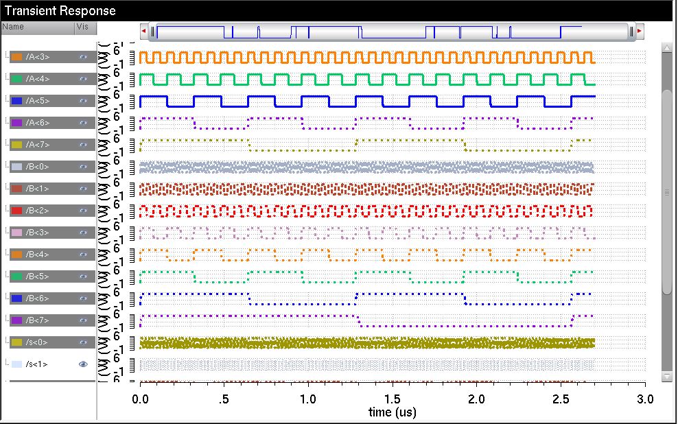
8_bit adder simulation:
stimulate
the 8bit adder.we will have 2^20 possible inputs because we have 2^8
possible values of A and the smae for B,.and if you notice cin has
another two possible values.so what should we do in order to overcome
this issue?I would suggest to create couple of inputs and
check if they work as we expect them to work.i put the cin to be ground
and i put a pulse sources to different pulse width and periods.and i
try to simulate them and see if i have a correct results,.although it
might not give you a correct anwer in the first place so go ahead
and chnage the pulse width until you get the correct results,.
I
ploted all of the inputs and outputs ,you can look at the traces
at one segment at the time.you should get something like this afetr you
seperate the traces:
My Design directory: "Here"
Return to EE 421Labs "Here"
Return to Mari Gilligan Labs "Here"