Lab
X - ECE 421L
Mari
Gilligan
Email:mgill19@unlv.nevada.edu
10-17-2015
We will go through the Tutorial 4 for our prelab :
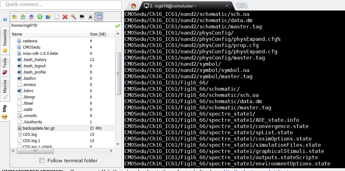
Back up your Ducumnets as usual:
in
order to creat the bakup,go to Moba-x term and log in to
Csimcluster.ee.unlv.edu, when you sign in type this sentence
(tar-cvf backupdate.tar CMOsedu/).
using
this commend will creat the tar file with all projects saved.after you
creat the tar file type this commond ( gzip backupdate.tar).this command helps us to have the back up dpcuments in smaller size file.
Luanch virtuoso;copy Lab5 to Lab6 in the Library manager,and click on the update instatnces when you are copying .
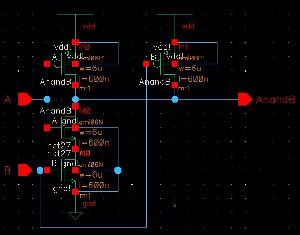
we
are going to have a Nand gate ,so will start by using the inverter from
lab 5,change the Pmos to 6.0u/6.0u and do the same for Nmos as
well.wire things up and you should have this schematic :
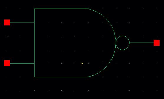
create the symbol view from your schematic and delete everything in it ,Like this:
simulation of the gate operation ,make a schematic view of a cell called sim_nand 2 and draft the following :
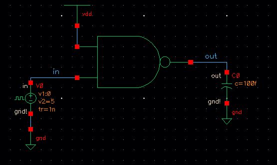
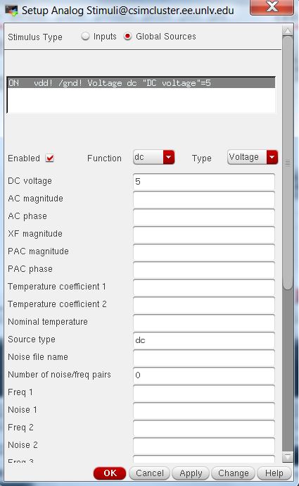
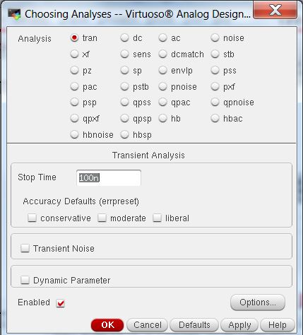
setting the source and the analysis as follows:
Note: If you are using Golobal stimuli ,you cany have a DC source as well
ADL->Model libraries->for setup Models.
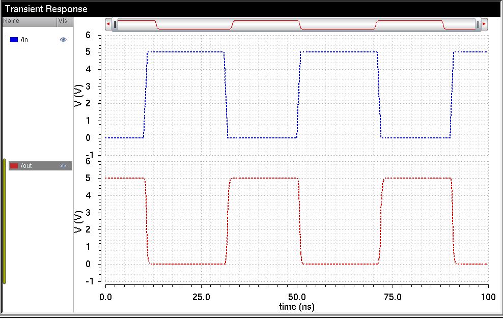
After setting ,check and save and run the simulation and you should get this:
Next
close nad save all the open cells ,Use Library manager to open the Nand
layout cell view ,which shows the invereter ,since we copied it at the
beginign
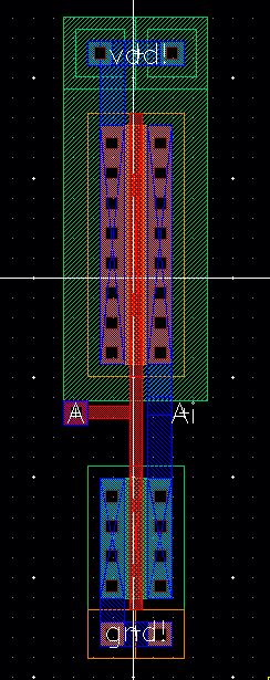
Get ride of the metal1 fron the Ntap to the source of the pmos and delete the vdd! pin.
copy the Pmos cell as seen below.
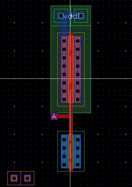
we
need to copy the Pmos in such a way that would overlap the left pmos
and then chnage the ntap cell,so that has 5 columns of contacts ,DRC
the layout.
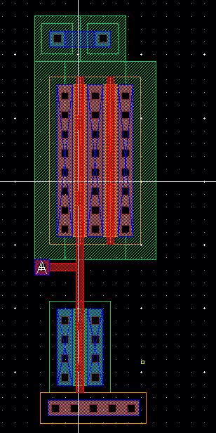
Next
move the ptap cell so its under the nmos cell,and then go ahead and
copy the nmos and overlap it with the first like we did for the nmos
.make sure the pin names are showing,.BPin is (input),and Vdd! and gnd!
are (inputoutput) .
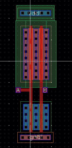
Since
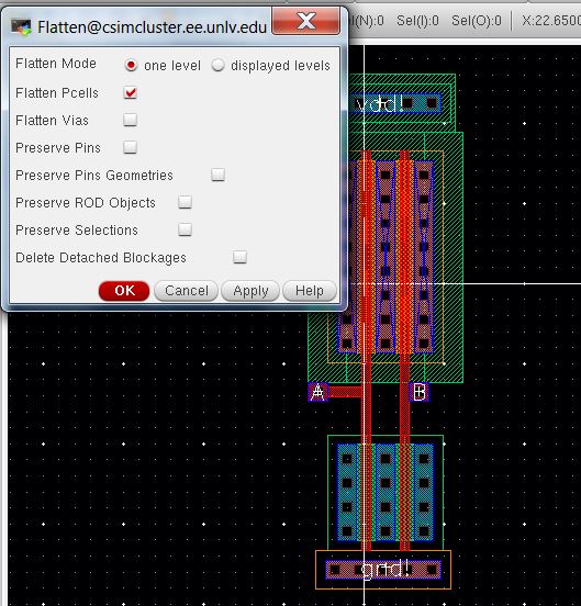
we notice we have the metal between the Mosfets that we dont need.
it,select both mosfets then flatten then (this will make the nmos cell
to be no longer cells but rather rectangles in the layout).
Deselect thet prevouse pins Geometrics.This will ensure that the goemetric information of flattend pins is not preserved.
we dont want pins or the pin information in our layout .
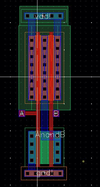
now
delete the metal1 and contacts between the two nmos.add the metal1 to
gnd! aand vdd! (two places) and conncet the drains of the two pmos to
the drain of the nmos.DrC your layout.
extract the layout and Lvs your layout:
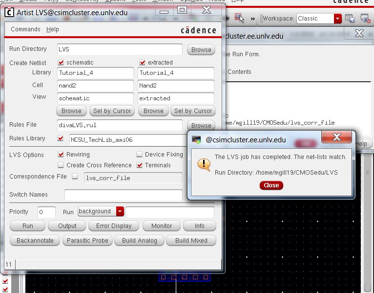
save and close everything.this concludes Tutorial4.
End of Prellab4
stimulation
of 2_Nand Gate ,by creating the new schematic view for the simulation
,we will be using two pulse inputs ,set your nmos and pmos to be
6.0u/6.0u for both .
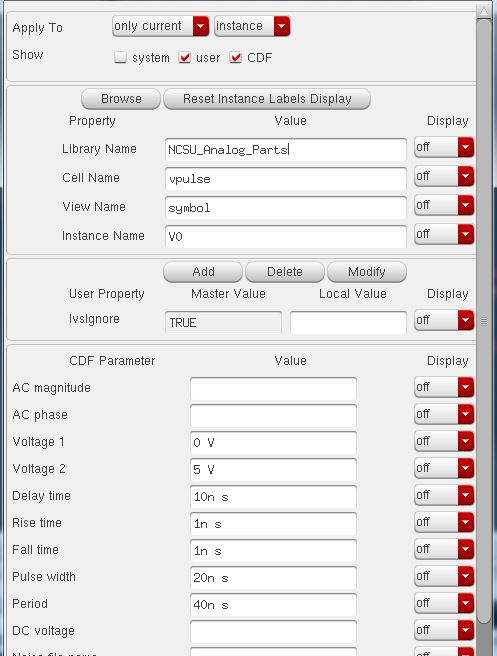
im using the 2_pulse to be mu inputs :
Launch the ADE_L and perform transiant analysis:
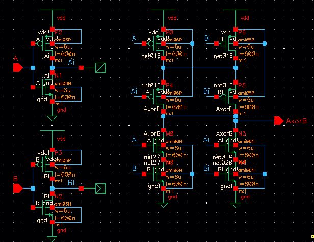
we need to reapeat above instructure for our XOR gate as well:
so start with creting your schematic first ,this process is a little complicated so make sure that pay close attention:
next step is to create the symbol:
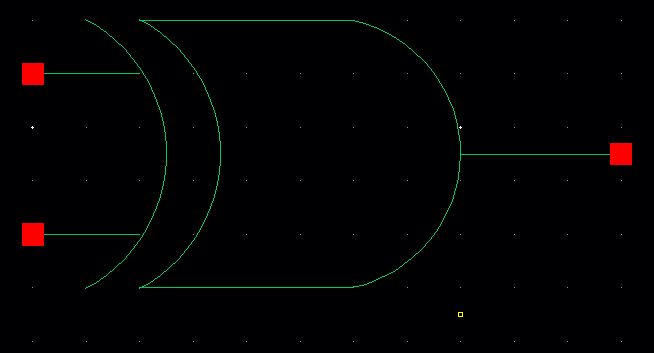
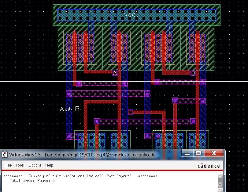
the most important part to creat the layout :
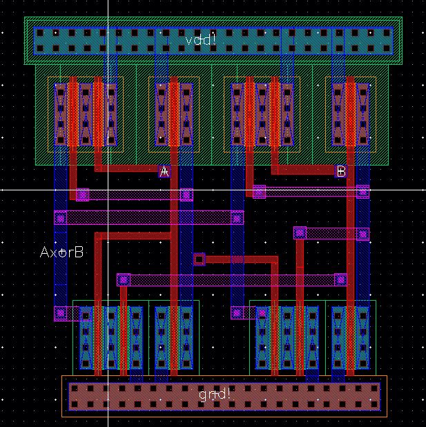
check and save and run the DRC on your layout:
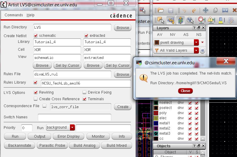
now we get the extracted from the layout by go to ->verify->extract:
then open the extracted view and run the LVS :
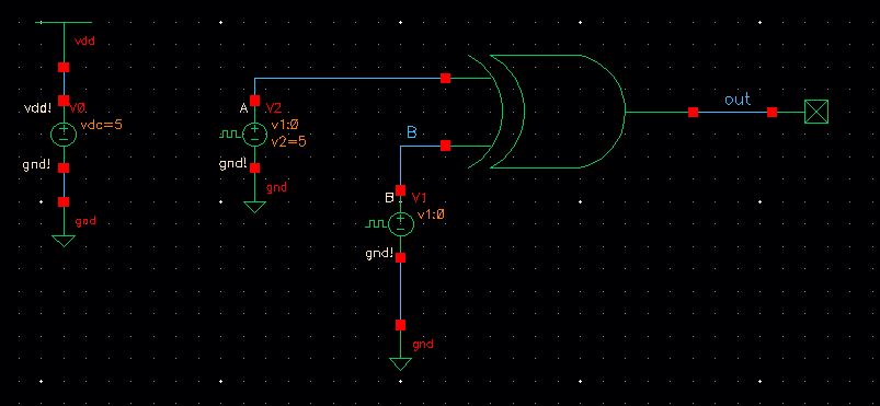
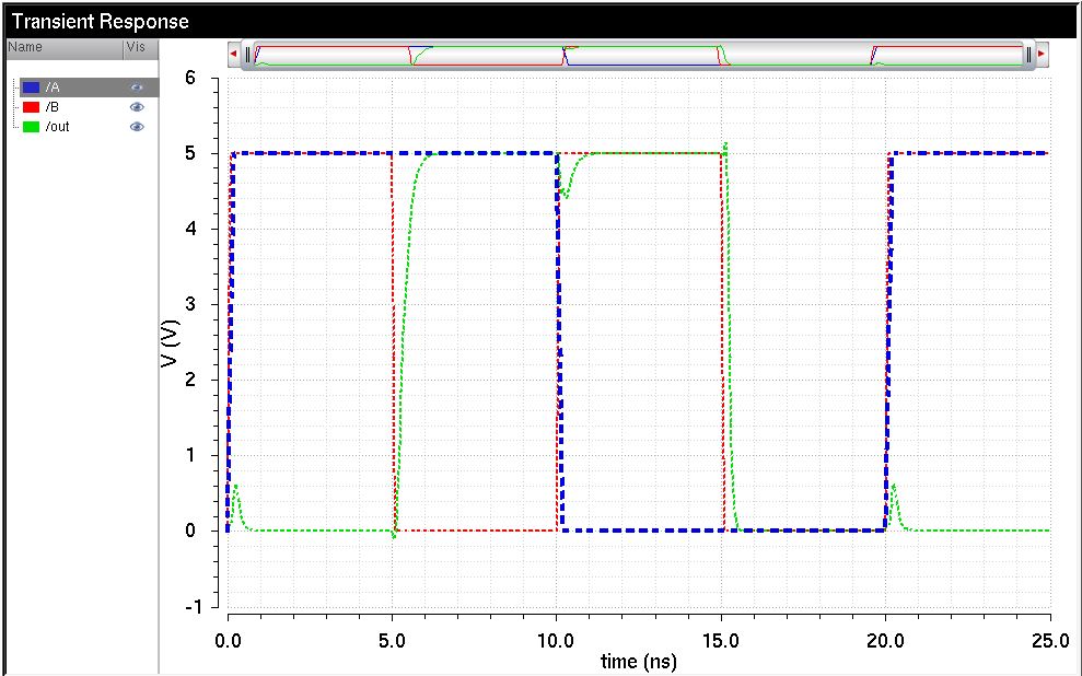
Next test the XOR gate like this by sing the Nand gate and run the transient Analysis:
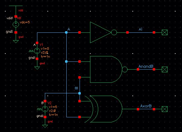
now
that we are familier with the process and Nand and XOR,we are going to
build the full adder,and should be similar to what i have here:
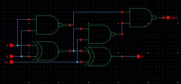
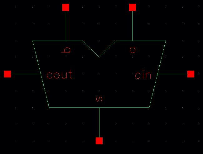
after we get the schematic we need to get the symol view as we alwyas do :
Layout of our Full adder:
ill
be using the metal2 for my conncetions and couple of pins,when you do
your layout you might have extra vdd nd Gnd on the top of each other,so
go ahed and delete the extra ones,.make sure your connction are correct
other wise you will get an error and since its a complicated process
,it might not be easy to see your maistkes,.
your layout should be like this:
check and save and run the DRC:
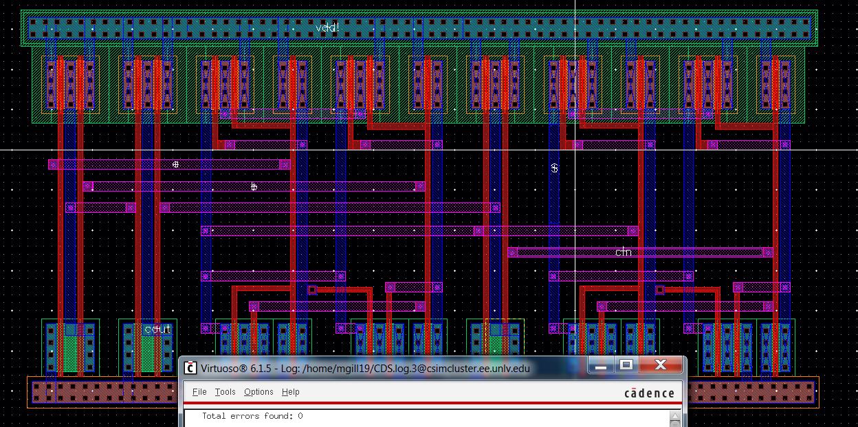
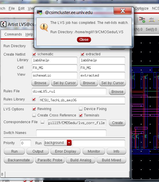
Run the LVS:
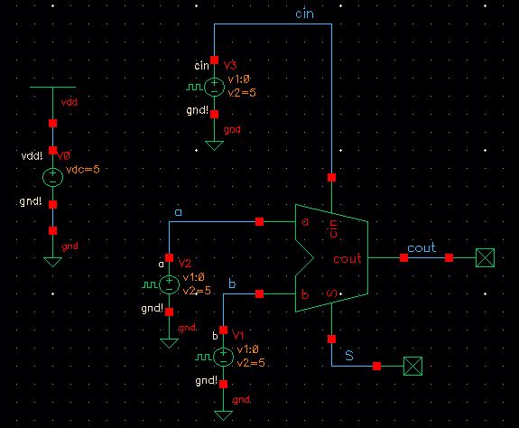
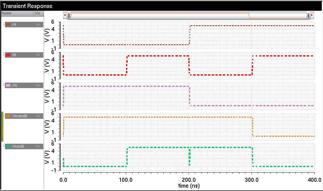
now your full adder need to simulate with 3input pulse sources:
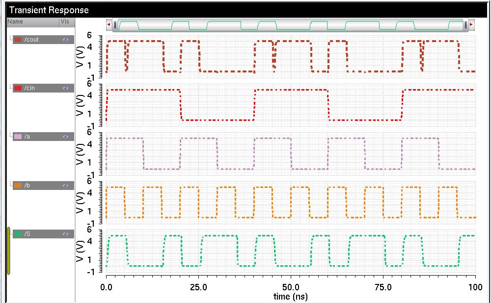
I try my Analysis for 100ns,And thats my simulation results.
now we need to simulate this schemtic:
Back up documnets "Here"
Return to EE421 Labs "Here"
Return to Mari Gilligan Labs "Here"