Project - EE 421L
Authored
by Steven Leung
Leungs@unlv.nevada.edu
11/4/15
Lab
description
The final project includes the schematics and simulations of the following circuits:
- Design of an 8-bit resettable (input "clear") up/down counter
- The outputs of your counter should be buffered before connecting to a pad
- A 31-stage ring oscillator with a buffer for driving a 20 pF off-chip load
- NAND and NOR gates using 6/0.6 NMOSs and PMOSs
- An inverter made with a 6/0.6 NMOS and a 12/0.6 PMOS
- Transistors,
both PMOS and NMOS, measuring 6u/0.6u where all 4 terminals of each
device are connected to bond pads (7 pads + common gnd pad)
- Note
that only one pad is need for the common gnd pad. This pad is used to
ground the p-substrate and provide ground to each test circuit
- Using
the 25k resistor laid out below and a 10k resistor implement a voltage
divider (need only 1 more pad above the ones used for the 25k
resistor)
- A 25k resistor implemented using the n-well (connect between 2 pads but we also need a common gnd pad)
25 K Resistor
Below are a few screenshots showing the schematic and simulations for a 25 k resistor.

25K Resistor schematic | 
Symbol created for 25k Resistor |

Simulation Circuit | 
Simulation Results |
I used a DC sweep from 0 to 5 V on one side of the 25k resistor to simulate the functionality of the reisitor. The
results are expected, there is no current through the resistor when the
source is 0 V and when the source is 5 V, there is 200 uA flowing
through the resistor.
Voltage divider
My
voltage divider includes a 25k followed by a 10k resistor. The
following pictures below show the schematic and symbol for a 10k
resistor.

10K Resistor Schematic | 
10K Resistor Symbol |
The
following picture is the schematic and simulation results for the 25k,
10k voltage divider. The input is 5 V and the expected output is
5*(10K)/(10K+25K) = 1.429V.

Voltage divider symbol
| 
Simulation Schematic |

Simulatoin results | |
NMOS Transistor
Below is the schematic, symbol along with IV characteristic curves for a 6u/.6u NMOS transistor.

Schematic for NMOS device | 
Simulation Circuit for NMOS Device |

ID Versus VDS (Stepping VGS) | 
ID Versus VGS |
PMOS Transistor
Below is the schematic, symbol along with IV characteristic curves for a 6u/.6u PMOS transistor.

Schematic for PMOS Device | 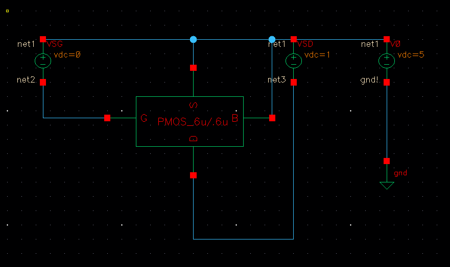
Simulation Circuit for PMOS Device |

ID Versus VSD (Stepping VSG) | 
ID Versus VSG |
Inverter with 6u/.6u NMOS and 12u/.6u PMOS
Below is the schematic and simulation of a 12u/6u inverter.

Inverter Schematic | 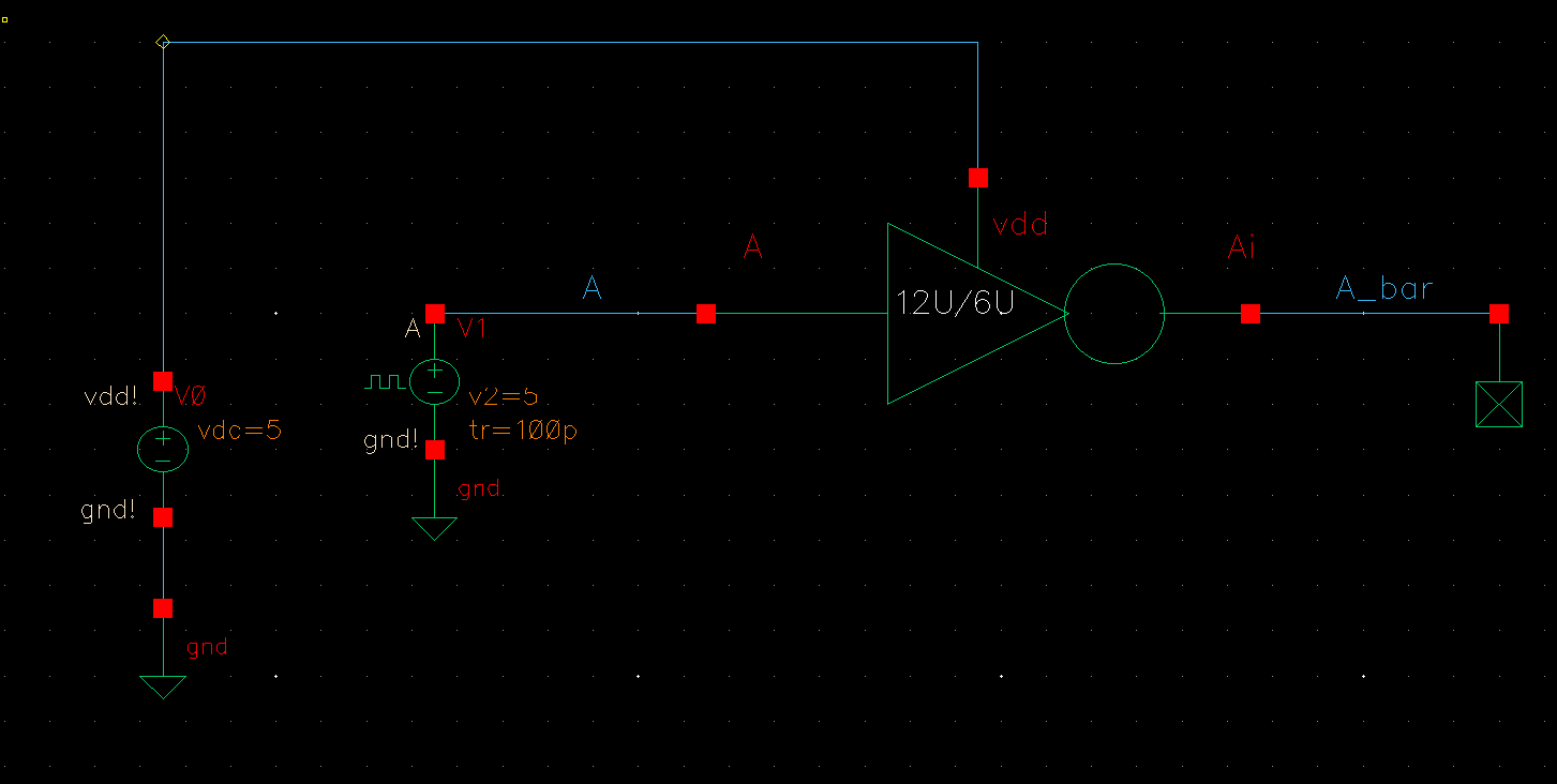
Inverter Symbol/Simulation Schematic |

Simulation Results | |
From
the simulation results, we can see that the output of the inverter is
inverted compared to the input at all times.
NAND/NOR gate with 6u/.6u transistors
Below is the schematics and simulations for bot the NAND and NOR gate.

NAND Gate Schematic | 
NOR Gate Schematic |

Simulation of NAND and NOR gate | 
Simulation Results |
The
simulation of the NAND and NOR gate consisted of feeding all 4 possible
combinations of the inputs to each gate (00,01,10,11). The results are
as expected, the only time tha tthe NAND output is low is when bot
input signals are high (11) and the only time that the NOR gate output
is high is when both inputs are low (00).
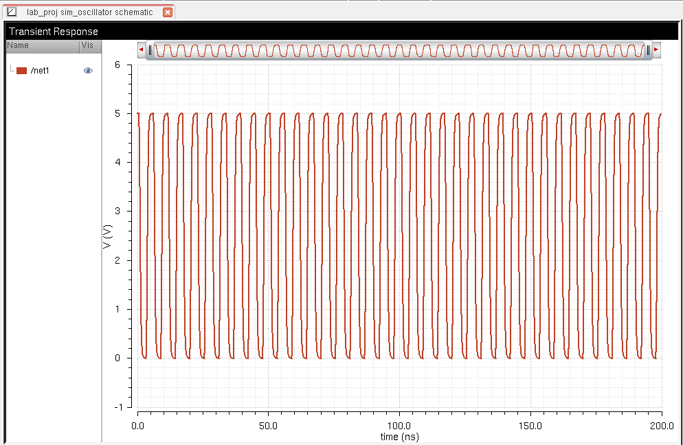
31 Stage Oscillator
Below
is the schematic and simulatino of a 31 stage ring oscillator with an
output buffer driving a 20pF load. The 2 inverters outside the inverter
array are used as an output buffer so that the oscillator can drive a
20pF load. From the simulation we cna see that period of the oscillator
is about 5ns which translates to a frequency of 200Mhz.
| Schematic | 
Simulation of Ring Oscillator |
Simulation Results | |
8-Bit Resettable Up/Down Counter
The
basic building block of a Resettable Up/Down counter is a D flip flop
with a clear. Below are the pictures showing a D flip flop with a clear
and the simulations.

Schematic of resettable DFF | 
Simulation Circuit for DFF |
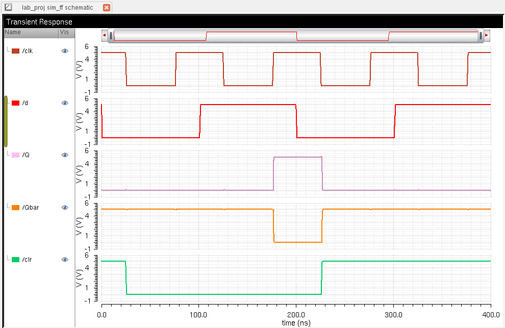
Simulation | |
Below are pictures showing the cells building upon the DFF to create an up/down counter.
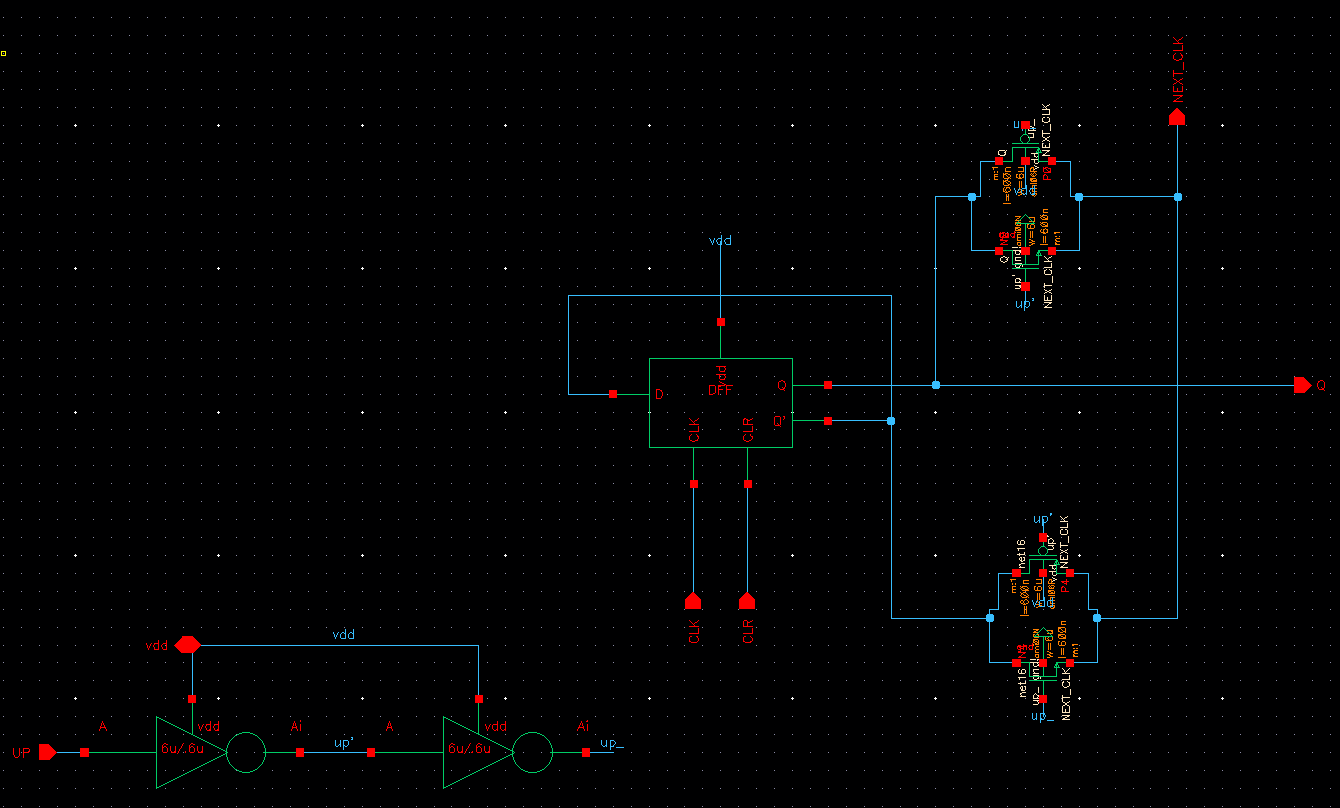
Single Bit of Up/Down Counter
| 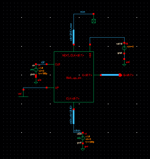
Schematic/Simulation of 8 Bit Up/Down Counter |
To
go from a single bit up/down counter to the 8 bit counter, simply
create a symbol for the 1 single bit and instantiate it 8 times. Then
create a symbol of the single bit instantiated 8 times go have a symbol
for a 8 bit up/down counter.
The
functionality of the up/down
counter is that when an input signal high (VDD) is fed into the
"UP" input, the counter will count up. When a input signal low (GND) is
fed into the "UP" input, the counter will count down. Also whenever a
high is fed into the CLR, the counter will clear all it's registers to
0 and start up or down counting from 0 once the CLR signal goes low.
Below are the simulations showing the counter counting up, down, and clearing.

Counter Counting up to 255 (largest possible value) |

Counter Counting Up and Down |
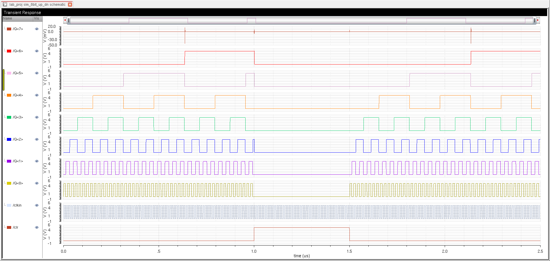
Counter Counting Up followed by CLR |
Below are the layouts to the cells shown above
Voltage divider

Voltage divider LVS |

Extracted (Showing the resistance values) |
NMOS/PMOS
| NMOS | PMOS |

NMOS LVS | 
PMOS LVS |

NMOS Extracted | 
PMOS Extracted |
Inverter

12/6 Inverter LVS |

12/6 Extracted |
NAND/NOR Gates
| NAND | NOR |

NAND LVS | 
NOR LVS |

NAND Extracted | 
NOR Extracted |
Ring Oscillator w/ 20pF buffer

Ring Oscillator LVS |

Extracted |
Up/Down Counter
Single flip flop

Flip Flop Layout |

LVS |

Extracted |
1 bit Up/Down counter

1 Bit Up/Down Layout |

LVS |

Extracted |
8 bit Up/Down Counter

Zoomed in 8 bit Up/Down Counter |

Full 8 bit Up/Down Counter |

LVS |

Extracted |
Link to design files here
Return to a listing of labs
Return to course web page
