Lab #8: MOSIS_chip4
Authored
by:
Brian Kieatiwong, kieatiwo@unlv.nevada.edu
Cassandra Williams, willi131@unlv.nevada.edu
Mari Gilligan mgill19@unlv.nevada.edu
Russ Prado, prador@unlv.nevada.edu
11/30/2015
Generating a Test Chip Layout for submission to MOSIS for Fabrication
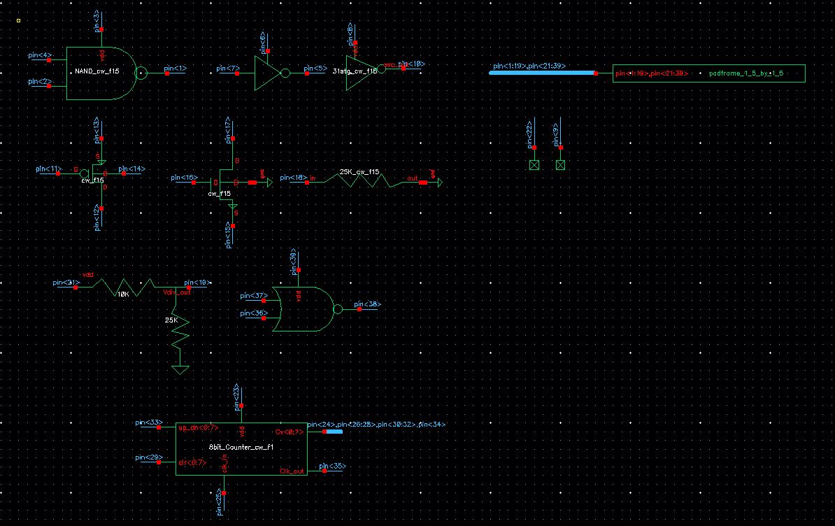
In this lab we are putting together a test chip that will be submitted for MOSIS fabrication.
The following structures will be included within this test chip:
- One up/down counter with clear
- The outputs of your counter should be buffered before connecting to a pad
- A 31-stage ring oscillator with a buffer for driving a 20 pF off-chip load
- NAND and NOR gates using 6/0.6 NMOSs and PMOSs
- An inverter made with a 6/0.6 NMOS and a 12/0.6 PMOS
- Transistors,
both PMOS and NMOS, measuring 6u/0.6u where all 4 terminals of each
device are connected to bond pads (7 pads + common gnd pad)
- Note
that only one pad is need for the common gnd pad. This pad is used to
ground the p-substrate and provide ground to each test circuit
- Using
the 25k resistor laid out below and a 10k resistor implement a voltage
divider (need only 1 more pad above the ones used for the 25k
resistor)
- A 25k resistor implemented using the n-well (connect between 2 pads but we also need a common gnd pad)
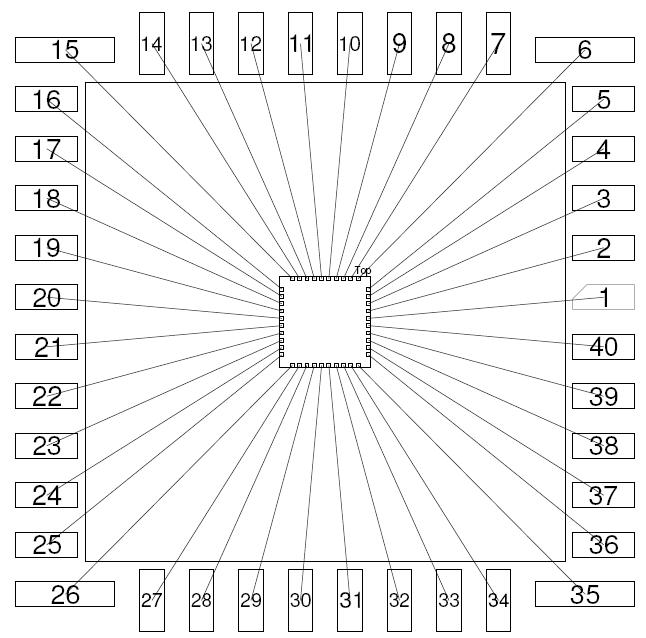
MOSIS_Chip4 Test Instructions:
- Up/Down Counter(8-Bit):
- To power is device, connect PIN<23> to a power supply
- With this counter, we can decide whether it will count up or down. With PIN<33>, a HIGH input will enable the counter to count up while a LOW input will enable a down counter.
- A Clear pin is also included in PIN<29>. With a HIGH input, we can clear all 8 outputs back to low, resetting the counter.
- A clock signal is needed at PIN<25> to begin the count.
- Outputs:
- S0=PIN<24>
- S1=PIN<26>
- S2=PIN<27>
- S3=PIN<28>
- S4=PIN<30>
- S5=PIN<31>
- S6=PIN<32>
- S7=PIN<34>
- 31-Stage Ring Oscillator:
- To power is device, connect PIN<8> to a power supply
- The output can be measured at PIN<10>
- NAND and NOR Gates:
- NAND Gate
- To power is device, connect PIN<3> to a power supply
- Input A is located at PIN<4>
- Input B is located at PIN<2>
- Output AnandB is located at PIN<1>
- NOR Gate
- To power is device, connect PIN<39> to a power supply
- Input A is located at PIN<37>
- Input B is located at PIN<36>
- Output AnorB is located at PIN<38>
- Inverter:
- To power is device, connect PIN<6> to a power supply
- Input A is located at PIN<7>
- Output Ai is located at PIN<5>
- Transistors(NMOS and PMOS):
- NMOS
- Gate is located at PIN<16>
- Body is already connected to the ground pin. Make sure that PIN<20> is connected to ground.
- Source is located at PIN<15>
- Drain is located at PIN<17>
- PMOS
- Gate is located at PIN<11>
- Body is located at PIN<14>. In order for this PMOS to avoid body effect, this pin should be connected to Vdd
- Source is located at PIN<13>
- Drain is located at PIN<12>
- MOSIS_Chip4 Padframe:Voltage Divider and Resistors(25k and 10k):
- 25K Resistor
- To test this resistor, use PIN<>. The other end of the resistor is already connected to ground at PIN<20>
- Make sure to connect PIN<20> to ground.
- 10k Resistor
- Voltage Divider
- Input pin is located at PIN<21>
- Output pin is located at PIN<19>
The simulations for each of these devices can be found at Lab Project
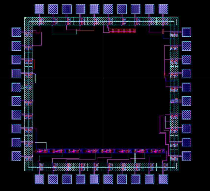
MOSIS_Chip4 Padframe:
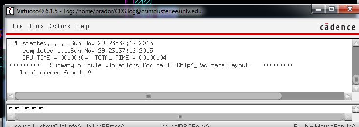
The image above shows how Lab 8 work is to be zipped and emailed to myself for backup.
To download the cells from this lab, click here
Return EE421L Labs