
Lab 7 - ECE 421L
Go through Cadence Tutorial 5 on how to design and layout a ring-oscillator here
Buses can be created by pressing Shift+W
This lab will be making use of arrayed symbols in order to
make schematics more concise.
4-Bit Inverter
A 4-bit inverter would normally be instantiated by putting down 4 inverters and creating 4 input and output pins b<i> and bi<i> as shown below.

We can make a simpler equivalent schematic by naming one inverter “I0<3:0>” and routing buses to its input and output pins, which are denoted using the same notation ( b<3:0> and bi<3:0>).

Create a symbol and display text that indicates that it is a 4-bit inverter.

Create a simulation schematic for it. The four inputs are tied together to a pulse source. The outputs are connected to various capacitive loads.

Smaller capacitive loads have shorter rise and fall times. Larger loads have longer rise/fall times and more delay. This can potentially cause glitches in the output which can be seen in some of the later simulations.

8-Bit Gate Arrays
Modify the 4-bit inverter schematic to turn it into an 8-bit by changing the instance and pin names to have “<7:0>” appended to them instead of “<4:0>”.

Create schematics and symbols for an 8-bit input/output array of: NAND, NOR, AND, and OR gates. Implement them in a similar fashion as the 8-bit inverter. The AND gate is shown as an example. The implementation of the other gates will be identical.


Create a schematic to simulate the operation of the gate arrays.

AND

OR

NAND

NOR


8-Bit Wide MUX
Create and simulate a 2-to-1 MUX/DEMUX and symbol. Include an inverter in the schematic to invert the select bit.


The simulation shows that when the select bit is low it passes the value of input B and when high it passes input A. It also de-multiplexes the output into the many inputs.

Create an 8-bit wide MUX/DEMUX using the same method as with the 8-bit Gate arrays.

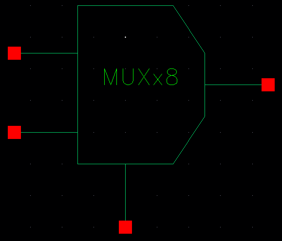
Verify with a simulation

8-Bit Adder
Create a schematic of the following CMOS And-Or-Invert (AOI) implementation of a 1-bit full-adder using 6u/0.6u MOSFETS and a symbol. The benefit of this implementation is that it significantly reduces delay.


Create a schematic and symbol of an 8-bit adder using the symbol of the previous 1-bit full-adder. Link the 1-bit adders together by routing carry out of an adder to the carry in of the next.


Simulate the 8-bit adder. From the results below you can see how the AOI implementation has reduced delay and minimized output glitches.


Example Check:
Fourth addition (time 300ns to 400ns):
A: 10011011 = 155
B: 01101110 = 110
Sum: 00001010 = 10
Carry In/ Carry Out: 1
Sum w/ Carry: 100001010 = 266 (in decimal)
Layout the 8-bit adder. Shown are the two most significant bits of the adder.

DRC and LVS.


Backup:
Cadence files and lab report are automatically backed up in my Dropbox folder.


The cadence files can be found here: lab7_jh.zip
Return
to the directory listing of students in EE 421L, Fall 2015