
Lab 4 - ECE 421L
Layout and simulation of NMOS and PMOS devices.
Create a schematic for simulating ID vs. VDS for the 6u_600n NMOS device. Instantiate an NMOS_IV from the NSCU_Analog_Parts > N_Transistors library and wire up two DC voltage sources. Have the body of the NMOS go to ground.
Create a simulation and click on the drain of the NMOS to select the current as an output.
In the Analyses menu, have VDS sweep from 0 to 5V with a step size of 1mV.

Create a variable called VGS. In Tools > Parametric Analysis set VGS to sweep from 0 to 5V with step size of 1V.

Run the analysis.

ID vs. VGS
Copy the previous schematic and change the value of V1 or VDS to 100m and V0 to 0 instead of VGS.

Run the sim and plot the current once again. This time have VGS sweep from 0 to 2V with step size 1mV.


ID vs. VSD
Create a schematic for simulating ID vs. VSD for the 12u_600n PMOS device. Have the body of the PMOS go to VDD.

Use the same steps used for setting up the simulations for the NMOS device for this one as well.

ID vs. VSG
Create a schematic for simulating ID vs. VSG for the 12u_600n PMOS device.

Here are the results.

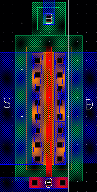
NMOS Layout
Create a schematic for the 6u_600n NMOS device, connected to four probe pads.

Layout the 6u_600n NMOS device by selecting the nmos
instance from the NCSU_Techlib_ami06 library.
Instantiate a ptap and connect it to the source and drain with metal 1. Also instantiate a via between m1_poly to connect the gate of the nmos. Create pins on metal 1 for gate, source, drain and gnd!

Connect all four terminals of the layout to probe pads using metals 1, 2 and 3. Make sure the layout DRC's and LVS's properly.


PMOS Layout
Create a schematic for the 12u_600n PMOS device, connected
to four probe pads.
Layout the 12u_600n PMOS device by selecting the pmos
instance from the NCSU_Techlib_ami06 library.
Instantiate an ntap and connect it to the nwell of the pmos. Also instantiate a via between m1_poly to connect the gate of the pmos. Create pins on metal 1 for gate, source, drain and base.
Connect all four terminals of the layout to probe pads using metals 1, 2 and 3. Check that it DRC's and LVS's.


Backup:
Cadence files and lab report are automatically backed up in my Dropbox folder.


The cadence files can be found here: Lab4.zip
Return
to the directory listing of students in EE 421L, Fall 2015