Lab 2 - ECE 421L
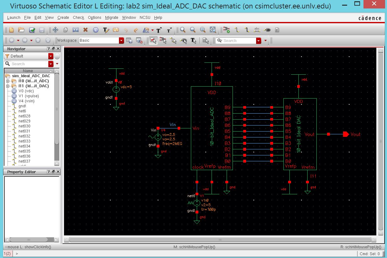
Design and create a schematic for a 10-bit ideal digital-to-analog (DAC) converter
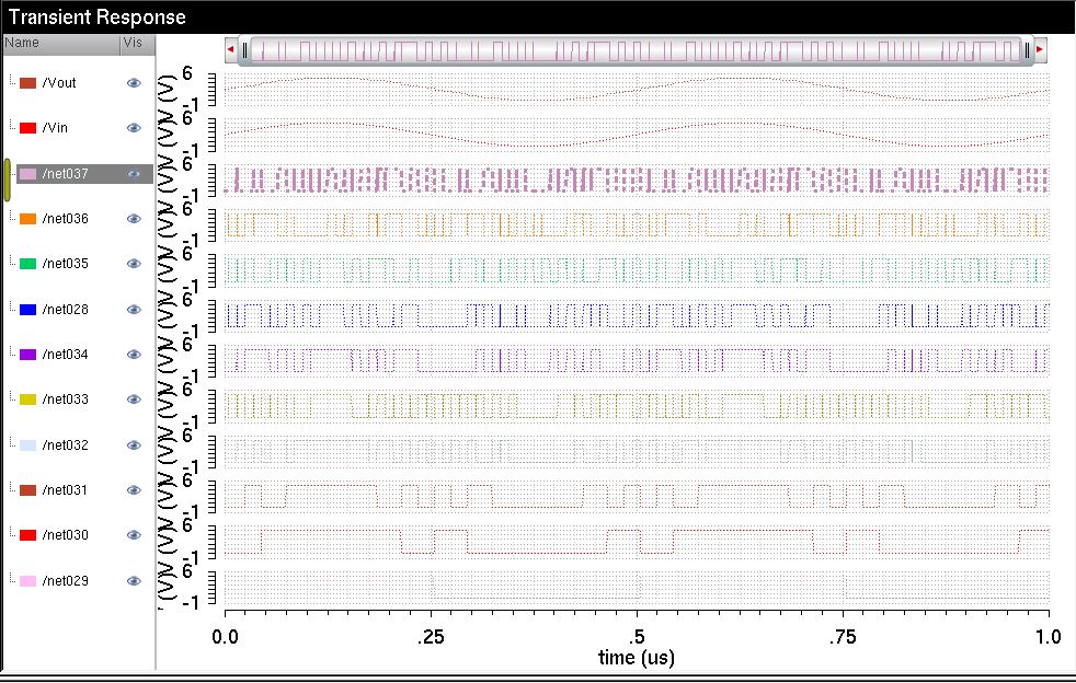
Run the Simulation: The output voltage forms a step-like wave around the input voltage signal, signifying its digital properties. One period of the square wave, representing the MSB of the digital signal, matches up with one period of the analog signal. The line colors and thicknesses of the traces have been adjusted for clarity.
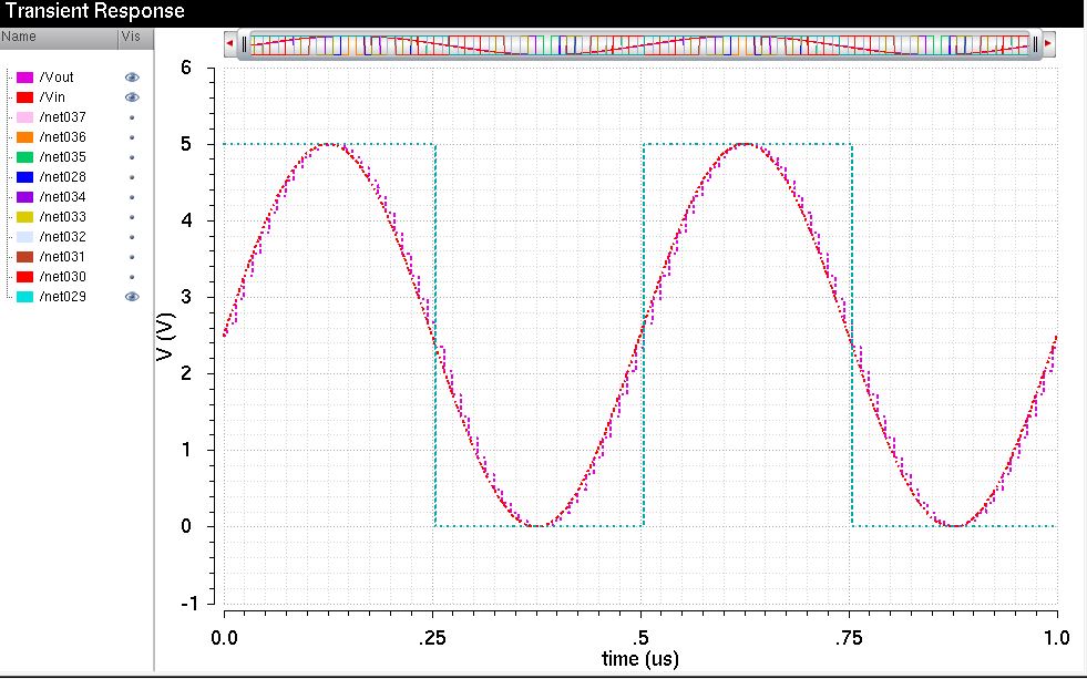
The period and amplitude of the simulation results will differ based on the analog signal that the ADC is given. The analog signal is converted to a digital signal by the adc and is then converted back by the DAC. The individual bits of the digital signal are shown here, with the LSB on net 37.
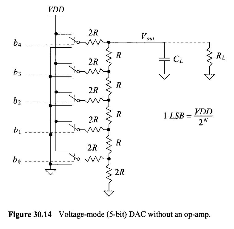
Design a 10-bit DAC using an n-well resistor of 10k ohms.
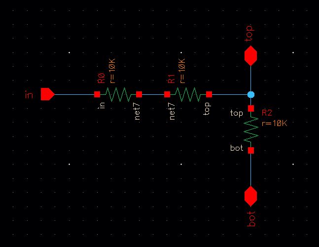
Design one bit of the DAC consisting of two 10k resistors in parallel with a single 10k resistor.
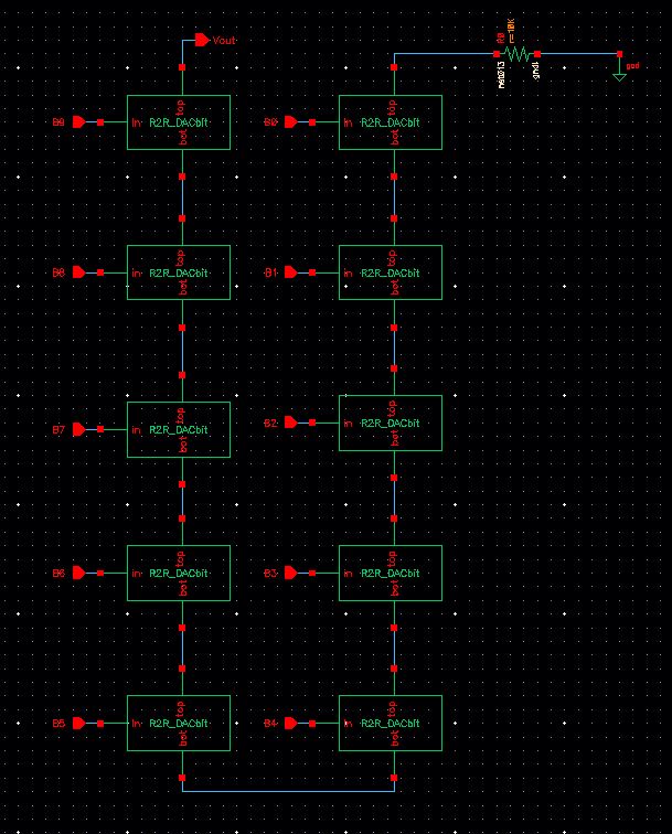
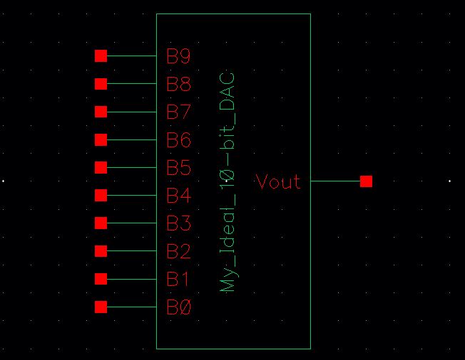
The final schematic of the 10-bit ideal DAC.
Determine the output resistance of the DAC:
The LSB of the resistor bridge has 2R (R=10k) resistors in parallel with another 2R. Their equivalent resistance is.
That R is combined in series with the R of the next bit in the ladder to create another set of parallel 2R resistors, yielding an equivalent resistance of R. This continues all the way to the output, resulting in an output resistance of R for the the DAC.
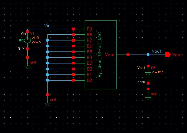
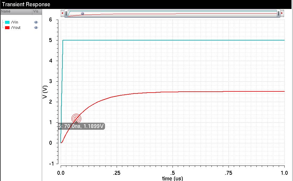
Predict the delay of the DAC while driving a 10pF load:
-by grounding all of the inputs and and connecting the MSB to a pulse source.
Creating a schematic symbol:
Copy the symbol from the original ideal DAC symbol file and delete the now unused VDD, Vrefp, Vrefm pins.
Simulations to verify correct operation of DAC:
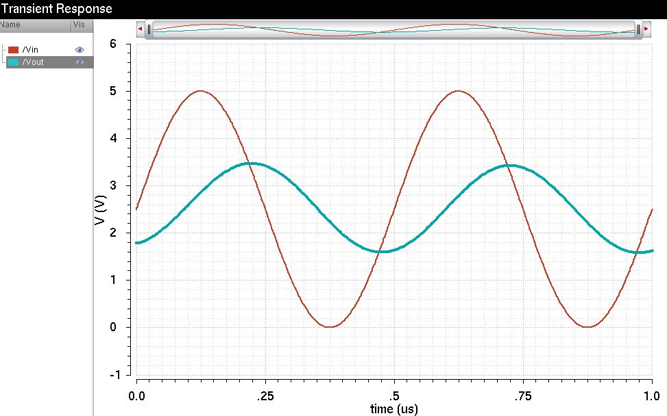
10k load: Since the output resistance of the DAC is R = 10k, we now have a voltage divider with two 10k resistors.
As the simulation shows, The output voltage is about half of the input voltage just as our calculations indicated.
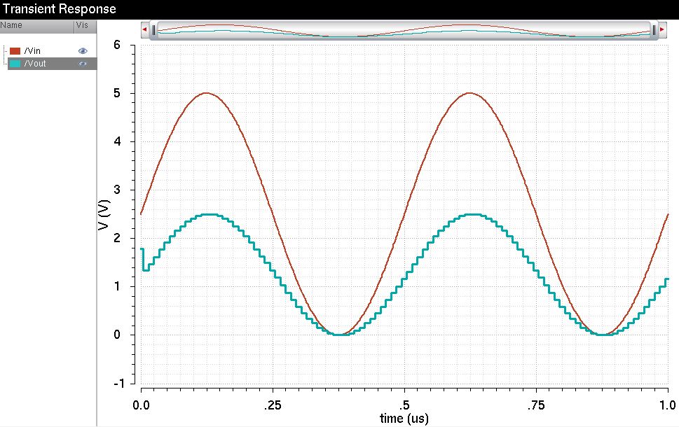
Rerun the simulation with just the 10pF capacitor. The output sine wave becomes smoother and is shifted about 100ns lagging the input.
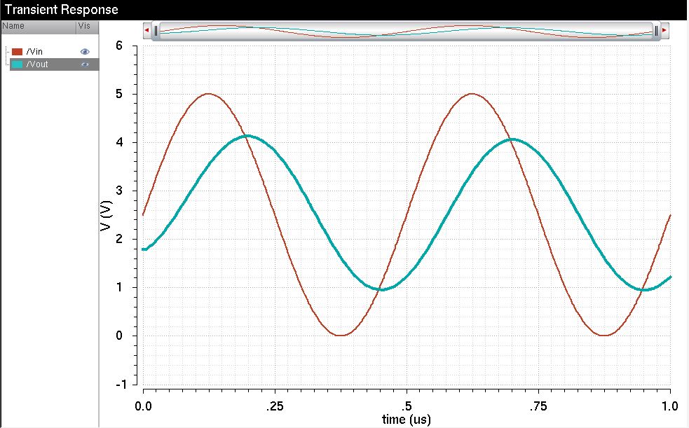
Rerun the simulation with both the 10k resistor and 10pF capacitor RC load. The output voltage is approximately 3.5V and 100ns lagging the input.
Resistance of Switches in a Real Circuit:
In a real circuit where the switches are implemented with transistors and are relatively large compared to R, the equivalent resistance becomes:
The 2R is in series with the larger resistance created by the switches, resulting in larger equivalent resistance.  Thus, the output resistance of the DAC will also be
larger, which will result in a decrease in the output voltage Vout of the the DAC.

Backup:

Cadence files and lab report are automatically backed up in my Dropbox folder.