Lab 8
Final Project - ECE 421L
Chip6_F15
Pre lab
- Back-up all of your work from the lab and the course.
- Go through Cadence Tutorial 6 seen here.
- Read through the lab in its entirety before starting to work on it
-Test structures to be included:
- One up/down counter with clear
- The outputs of your counter should be buffered before connecting to a pad
- A 31-stage ring oscillator with a buffer for driving a 20 pF off-chip load
- NAND and NOR gates using 6/0.6 NMOSs and PMOSs
- An inverter made with a 6/0.6 NMOS and a 12/0.6 PMOS
- Transistors, both PMOS and NMOS, measuring 6u/0.6u where all 4 terminals of each device are connected to bond pads (7 pads + common gnd pad)
- Note that only one pad is need for the common gnd pad. This pad is used to ground the p-substrate and provide ground to each test circuit
- Using the 25k resistor laid out below and a 10k resistor implement a voltage divider (need only 1 more pad above the ones used for the 25k resistor)
- A 25k resistor implemented using the n-well (connect between 2 pads but we also need a common gnd pad)
NOTE: Each test circuit should have its own power but ground should be shared between the circuits!
Pad(20) serves as a common ground to all test structure!
Pad(40) serves as common VDD for electrostatic discharge (ESD) protection.
Pad(20) and Pad(40) should always be connected to ground and VDD, respectively, when using the chip.
Pad(20) serves as a common ground to all test structure!
Pad(40) serves as common VDD for electrostatic discharge (ESD) protection.
Pad(20) and Pad(40) should always be connected to ground and VDD, respectively, when using the chip.
Chip structure

| Test Structure | Total Pad Connections |
| Up/Down Counter | 21 |
| 31-Stage Ring Oscillator | 2 |
| NAND | 4 |
| NOR | 4 |
| Inverter | 3 |
| PMOS | 4 |
| NMOS | 3 |
| Voltage Divider | 2 |
The configuration of the padframe follows the bonding diagram below. All pins on schematic are labeled according to the pin numbers on the padframe.
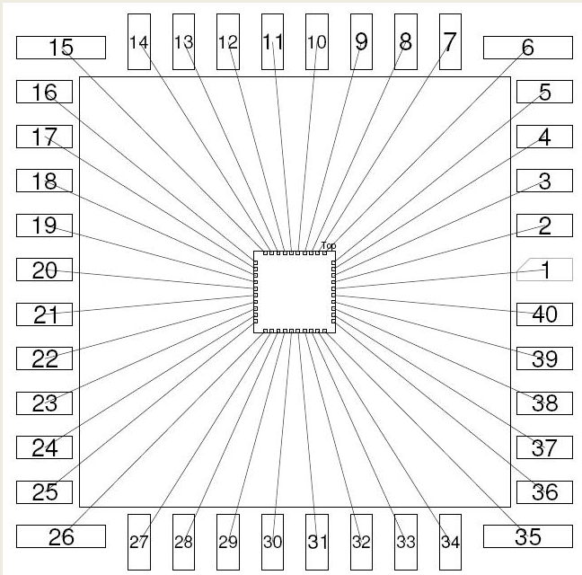
Full Chip Layout

Pin Assignment
We'll follow the bonding diagram up above to assign specific pad numbers to our structure pins.
All pad numbers are labeled from 1 to 40 (unless not used!).
Presettable Up/Down Counter with Clear Signal
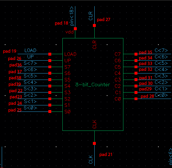
S<0-7> is the data to be loaded into the counter (7 = MSB, 0 = LSB)
C<0-7> is the current count (7 = MSB, 0 = LSB)
When CLR is high, the outputs of the counter will clear to 0.
If CLR is low and UP is high, the counter will count up.
If CLR is low and UP is low, the counter will count down.
Gates (NAND, NOR, NOT)
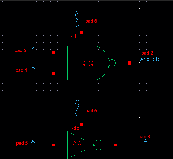
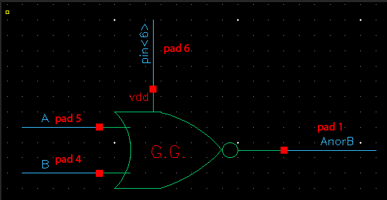
A and B are used as inputs to the gates (NAND, NOR, NOT).
All 3 gates use the same VDD (pad<6>).
MOSFETS (NMOS & PMOS) and Ring Oscillator

NMOS Size: 6u/0.6u
PMOS Size: 6u/0.6u
Ring Osc: 31 stage (approx 170 MHz)
Voltage Divider:
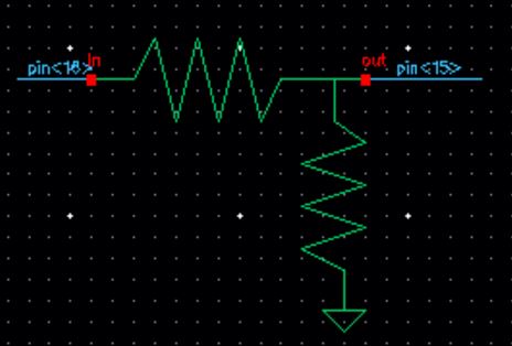
25k resistor between pad<18> and pad<15>
Vout = Vin (25k/(25k+10k))
Structure Connections and Testing
Voltage Divider

To measure the resistance of the 25K Ohm resistor, we probe pad(14) and pad(15).
To measure the output voltage of the voltage divider, we apply a known voltage to pad(16) and probe pad(15) using a multimeter to get the appropriate output voltage.

NMOS

Connect Drain to a fixed 5V power supply; pad(12).
Connect Source to GND; pad(11).
Connect Gate to an adjustable power supply; pad(13).
Increase the Gate voltage until current flows from Drain to Source. NMOS turns on when V(gate) is greater than V(threshold).
Connect Drain to a fixed 5V power supply; pad(12).
Connect Source to GND; pad(11).
Connect Gate to an adjustable power supply; pad(13).
Increase the Gate voltage until current flows from Drain to Source. NMOS turns on when V(gate) is greater than V(threshold).
PMOS

Apply a fixed 5V voltage to Source terminal; pad(9).
Connect Drain to GND; pad(7).
Connect Base to a fixed 5V voltage; pad(8).
Connect Gate to an adjustable power supply; pad(10).
When Gate is at 5V there's no current flowing from Source to Drain terminals. As the voltage from Gate is decrease below 5V - V(threshold), you'll get some current flowing and increases as Gate voltage drops.
NAND/NOR/INVERTER

NAND, NOR and Inverter share similar inputs; pad(5,4), but different outputs; pad(3,2,1).
-Testing NAND gate
Apply power to pad(16)
Apply square wave function generator to A and B inputs; pad(5,4), taken that 1 is high and 0 is low.
-Testing NAND gate
Apply power to pad(16)
Apply square wave function generator to A and B inputs; pad(5,4), taken that 1 is high and 0 is low.
| A | B | Out |
| 0 | 0 | 1 |
| 0 | 1 | 1 |
| 1 | 0 | 1 |
| 1 | 1 | 0 |
We'll get something similar when probing output at pad(2).
-Testing NOR gate
Apply power to pad(16)
Apply power to pad(16)
Apply square wave function generator to A and B inputs; pad(5,4).
| A | B | Out |
| 0 | 0 | 1 |
| 0 | 1 | 0 |
| 1 | 0 | 0 |
| 1 | 1 | 0 |
We'll get something similar when probing output at pad(1).
-Testing Inverter
Apply power to pad(16)
Connect a square wave function generator to pad(5) as input to the inverter. Ensure pad(4) is grounded because it is the input for the gates that share VDD with the inverter (if it is not grounded, the gates would be drawing power even when not in use).
Use an oscilloscope probe to determine the output of our inverter; pad(3).
-Testing Inverter
Apply power to pad(16)
| A | Out |
| 0 | 1 |
| 1 | 0 |
Connect a square wave function generator to pad(5) as input to the inverter. Ensure pad(4) is grounded because it is the input for the gates that share VDD with the inverter (if it is not grounded, the gates would be drawing power even when not in use).
Use an oscilloscope probe to determine the output of our inverter; pad(3).
Ring Oscillator

Connect power to pad(17) to power up our ring oscillator. We'll then use an oscilloscope probe to determine the oscillation frequency and time delay through pad(14).
Connect power to pad(17) to power up our ring oscillator. We'll then use an oscilloscope probe to determine the oscillation frequency and time delay through pad(14).
Up/Down Counter

Our counter has 21 inputs with clear and load which is fully programmable. That is, the value of the counter can be cleared to zero or preset to any value desired. When 'Load' is high, the data from our input pins are loaded into the counter.
Connect pad(18) to 5V to power up the counter.
Our counter has 21 inputs with clear and load which is fully programmable. That is, the value of the counter can be cleared to zero or preset to any value desired. When 'Load' is high, the data from our input pins are loaded into the counter.
Connect pad(18) to 5V to power up the counter.
DRC and LVS Check
Before we conclude our Final Lab for submission. Let's make sure everything work properly!
DRC check
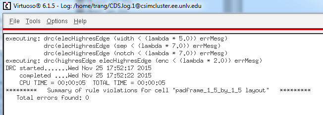
LVS Check
