Lab description
The purpose of this lab was to use wires in order to create arrays of gates.
Pre lab
- Back-up all of your work from the lab and the course.
- Go through Cadence Tutorial 5 seen here.
- Read through the lab in its entirety before starting to work on it
Lab Report
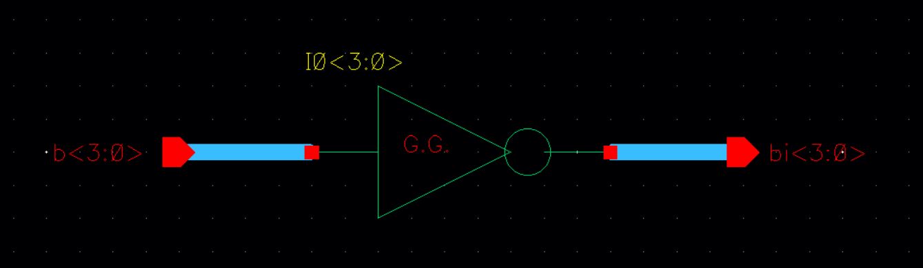
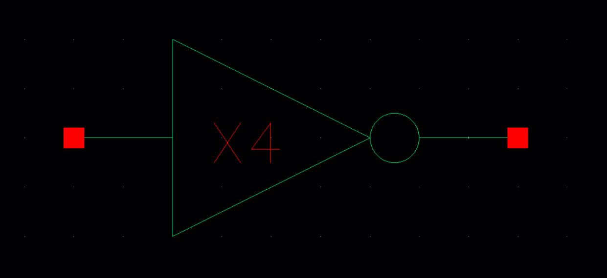
4-bit Inverter
- To understand how to make arrays of gates using buses we created a 4-bit inverter.
- The schematic was created with the inputs and outputs as seen below.
- A symbol was also created from the schematic.
- The schematic created was then simulated driving 100fF, 500fF, 1pF and no load.
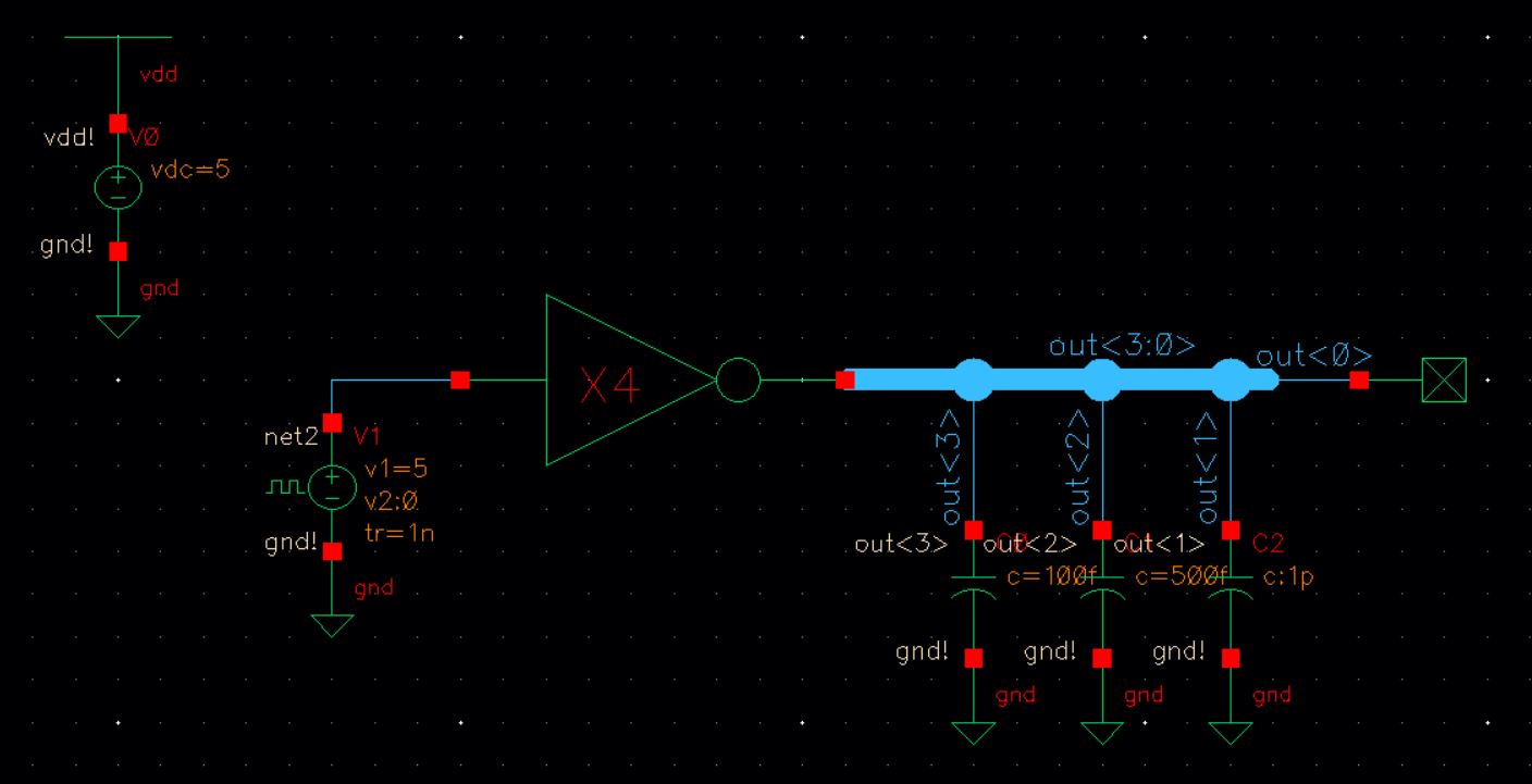
- The results obtained can be seen below.
- For the simulation with no load the delay of the output is minimal, but as the capacitance load gets larger the delay gets larger as well.
- This is because the inverter is not able to supply enough charge to the load.

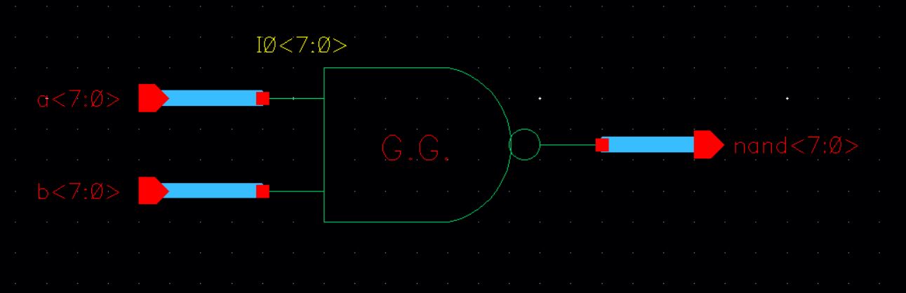
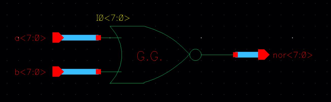
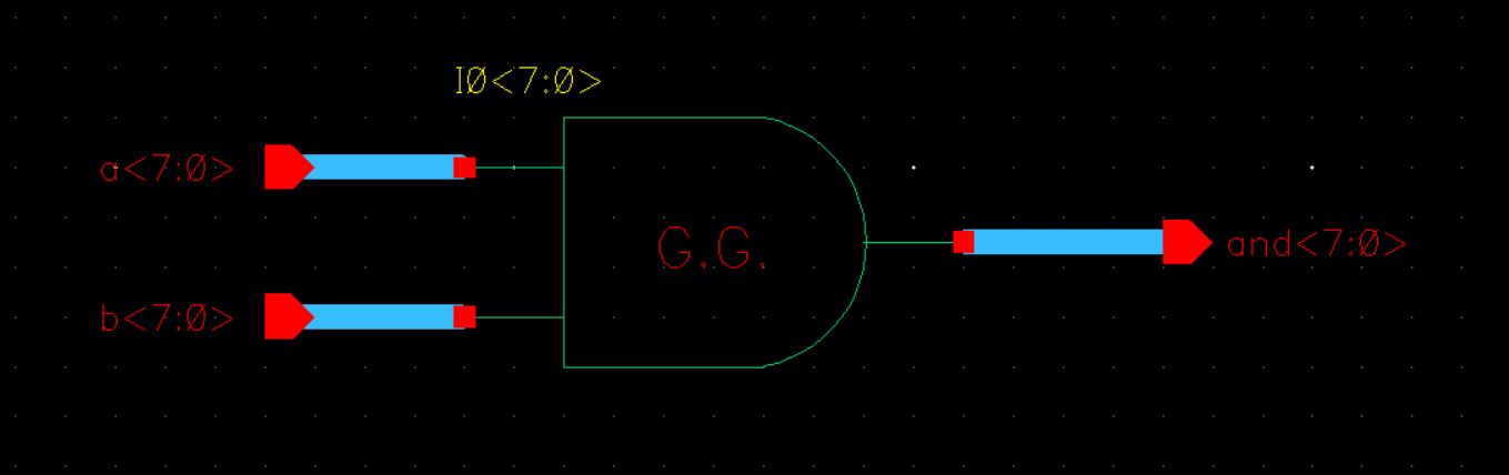
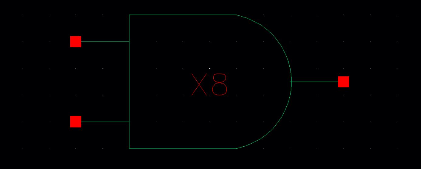
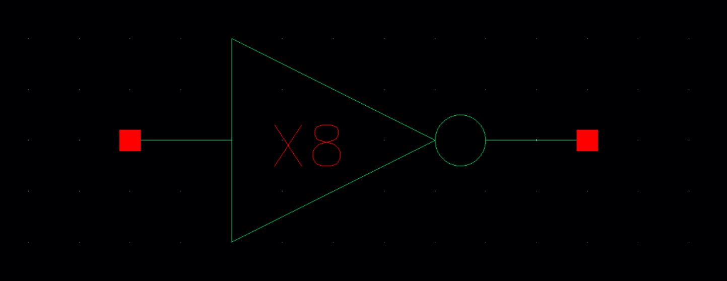
8-bit gates
- The same process was done to make an array of various 8-bit gates.
- An array of 8-bit NAND gates and a symbol were created as seen below

- An array of 8-bit NOR gates and a symbol were created as seen below

- An array of 8-bit AND gates and a symbol were created as seen below
- An array of 8-bit Inverter gates and a symbol were created as seen below

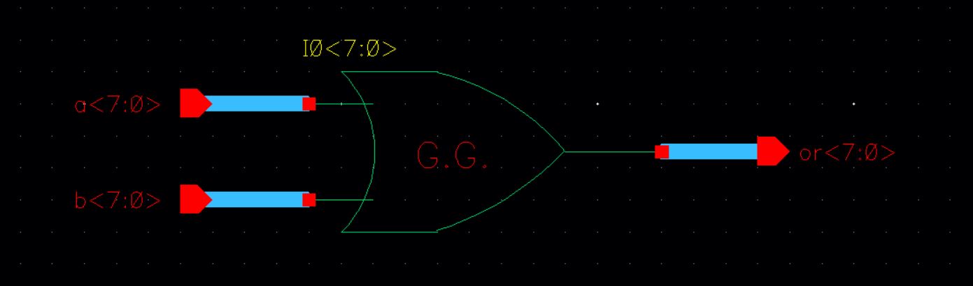
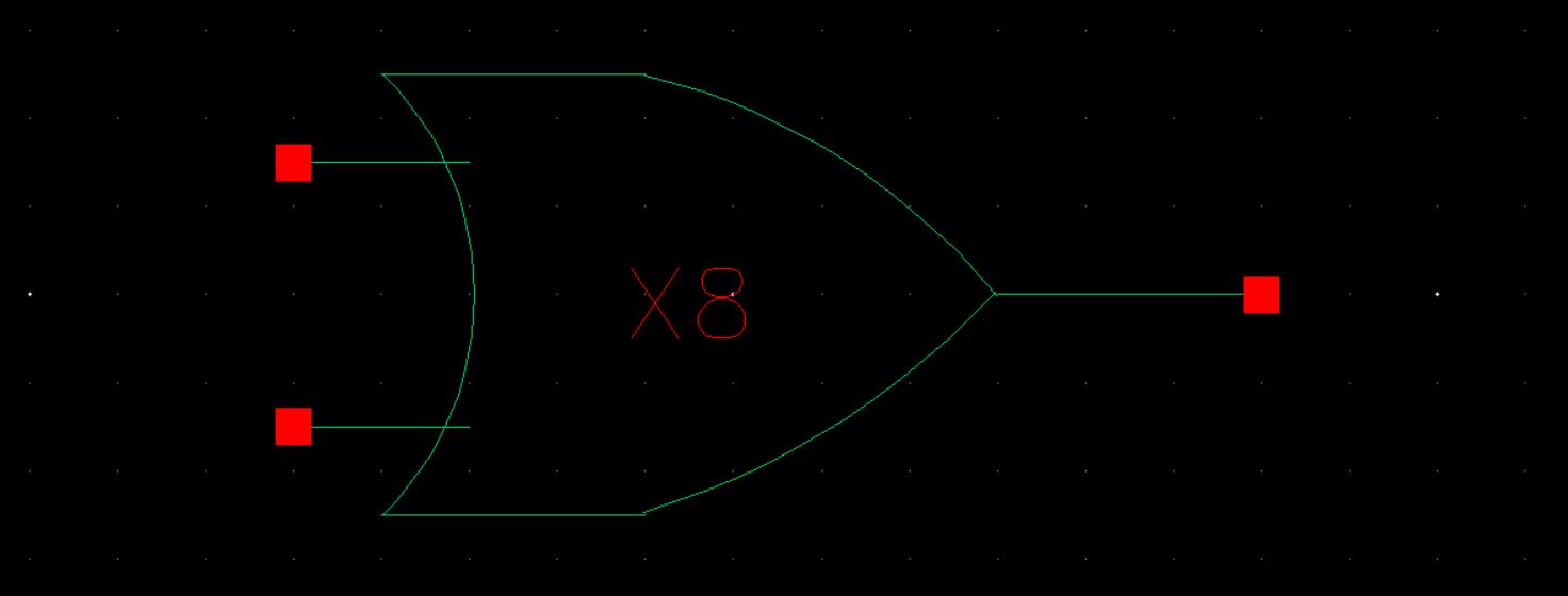
- An array of 8-bit OR gates and a symbol were created as seen below
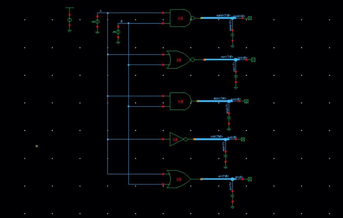
- A scheamtic was then created to test the operation of the 8-bit gates.
- To test them I took the output of 2 of the 8 possible outputs and connected one of them without a load and the other with a 1pF load.
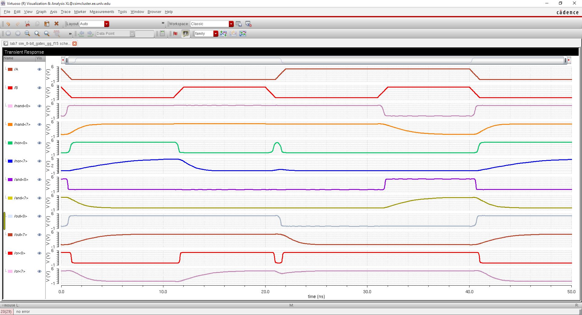
- The results obtained can be seen below which shows that the outputs for the same gates are the same just one of them has large delay from the large capacitor attached to it.
- Click on the image to see the simulation larger.
MUX/DEMUX
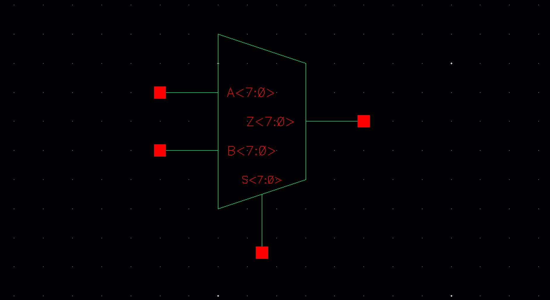
- A schematic and a symbol were then created for a 2 to 1 MUX.


- A schematic was then created to simulate the operation of the 2 to 1 MUX.

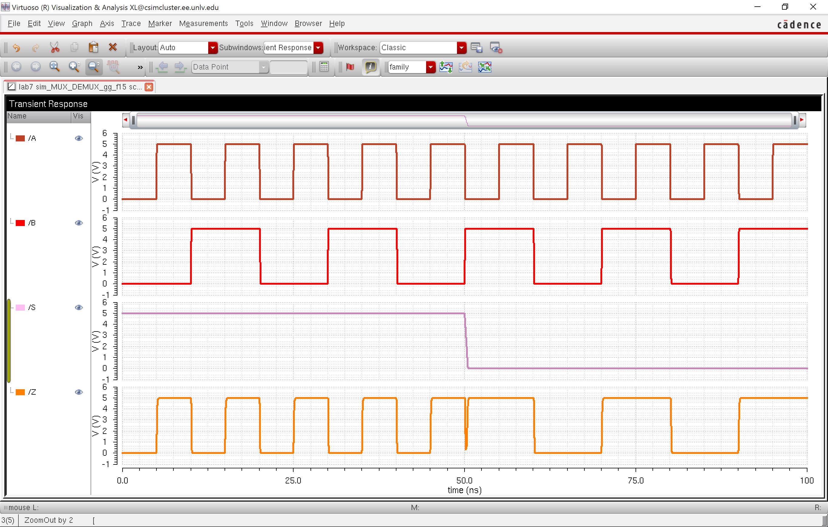
- The results obtained can be seen below.
- When the select line goes high the output will become the same as what is being input into pin A.
- When the select line goes low the output becomes the same as what is being input into pin B.
- The symbol was then used to simulate a DEMUX by switching our inputs and our outputs as seen on the schematic below.

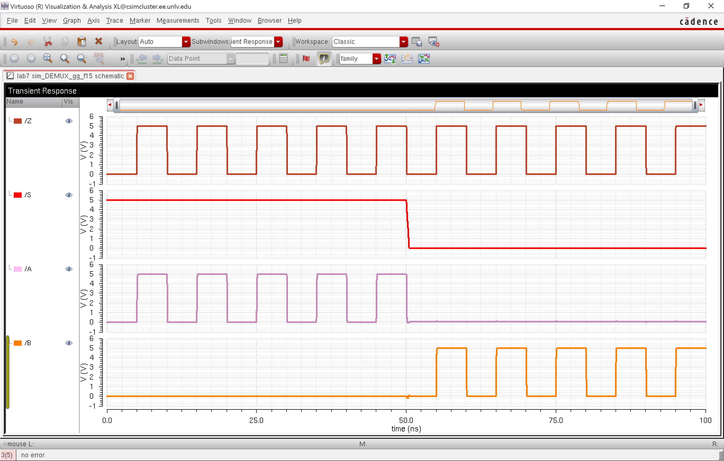
- The results obtained can be seen below.
- When the select line goes high the output A becomes the same as what's in the input, Z.
- When the select line goes low the output B becomes the same as what's in the input, Z.
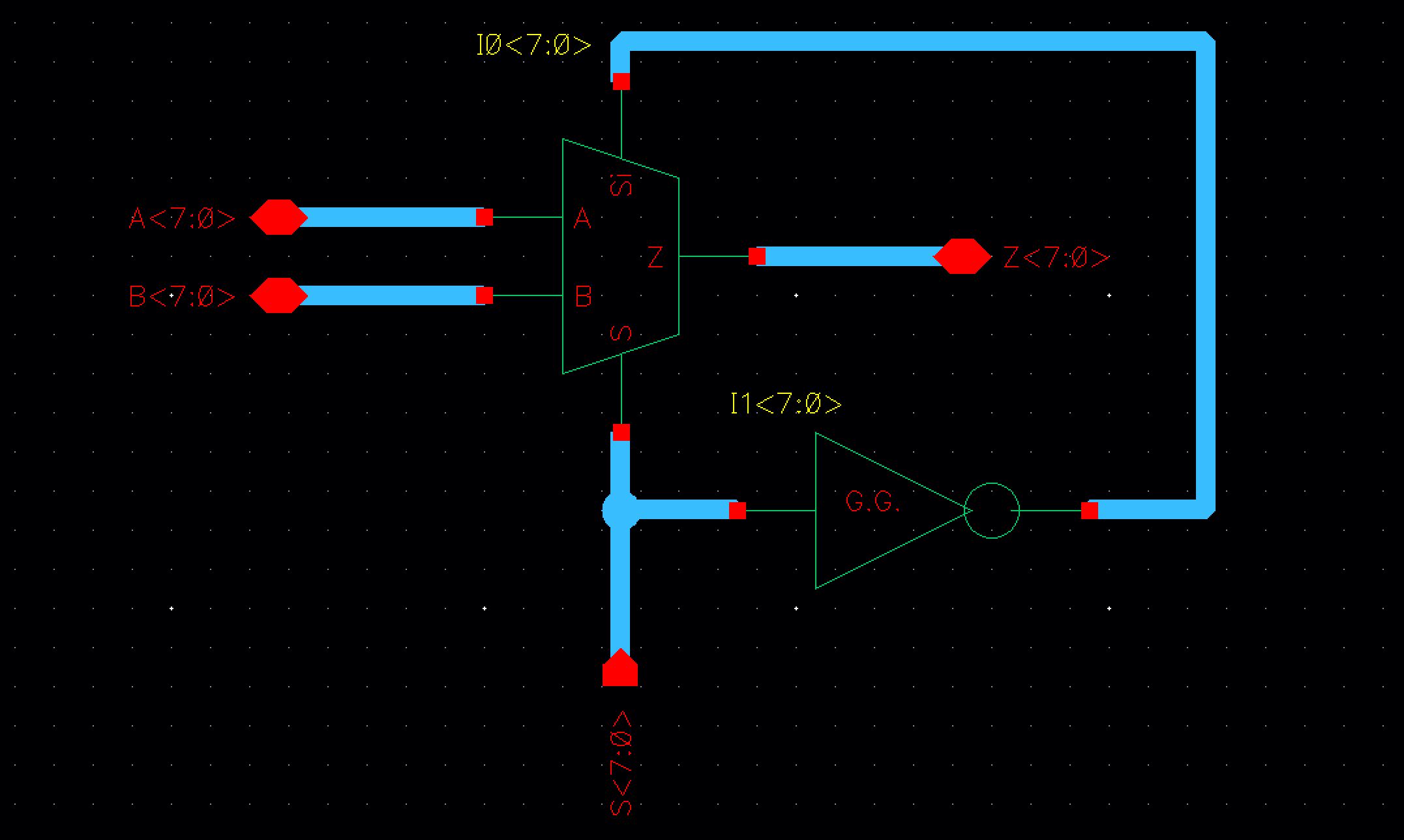
- The 2 to 1 MUX created before was then used to create an 8-bit 2 to 1 MUX.
- In order to be able to only need one select line an inverter was used inside it.
- A symbol was also created for this schematic.
- A schematic was then created to simulate the operation of the 8-bit MUX.
- To simulate we use 3 of the different MUXs in the array and check their operation.
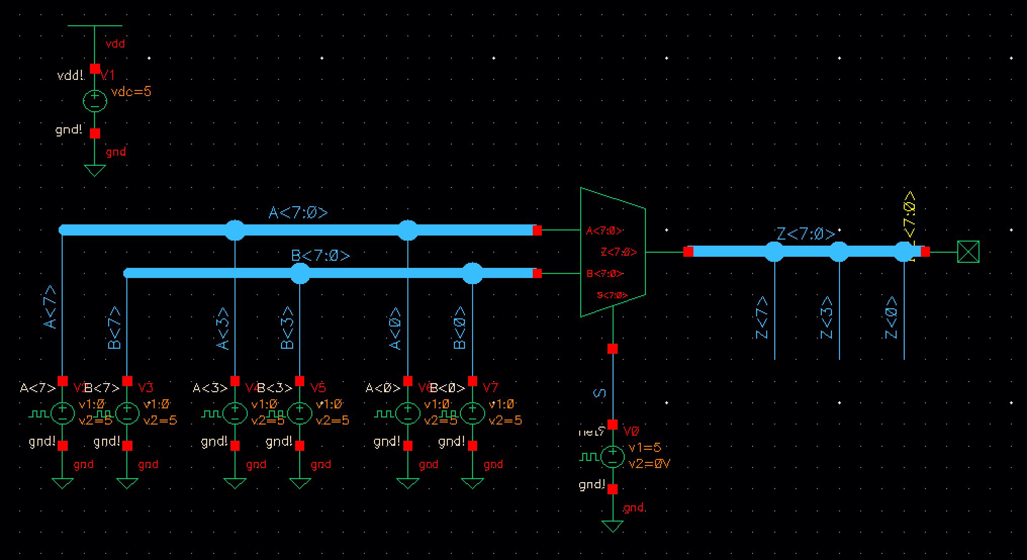
- The results obtained can be seen below.
- The behavior for each of the MUXs is what is expected.

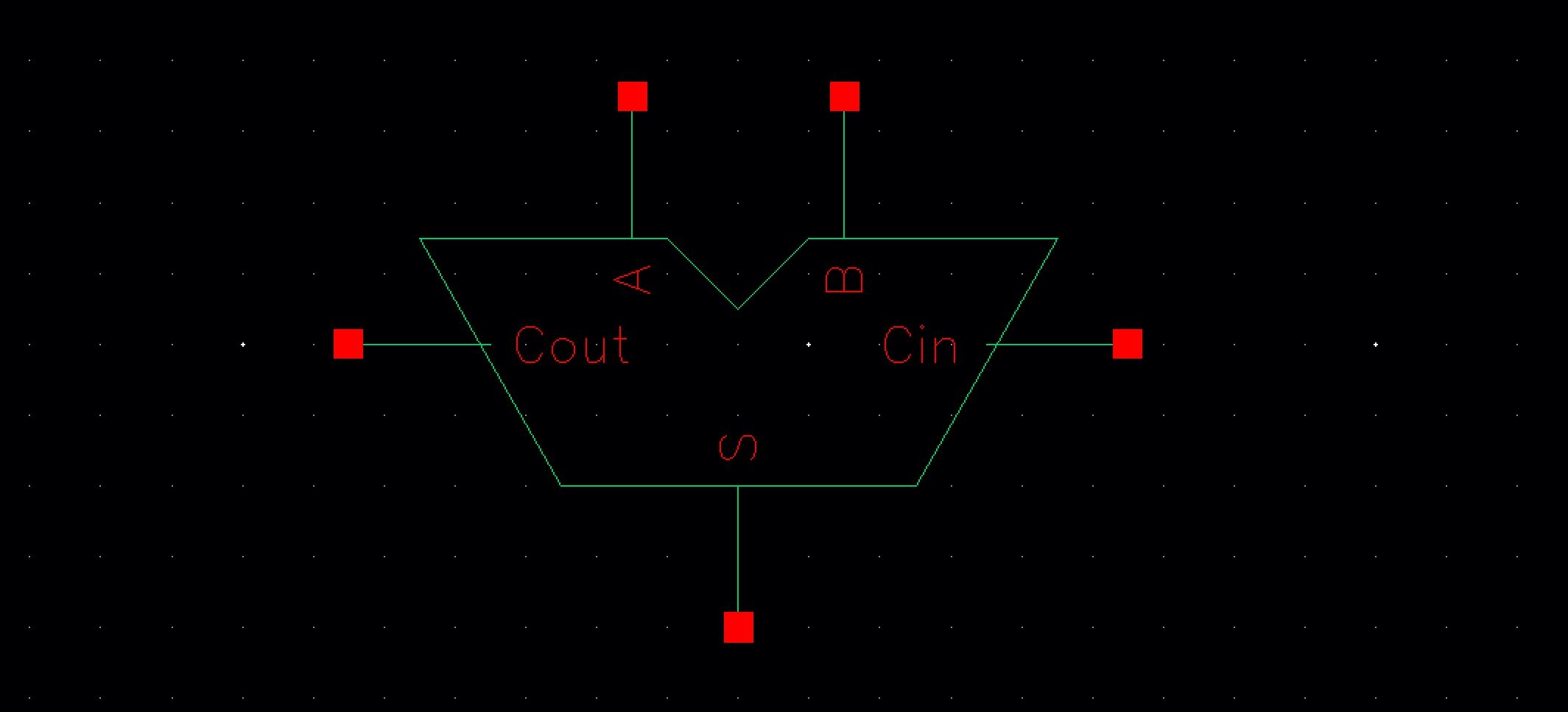
Full adder
- A schematic for a 1-bit full adder was then created following figure 12.20 of the book
- A symbol was also created for this schematic.

- A layout was then created for the 1-bit full adder.
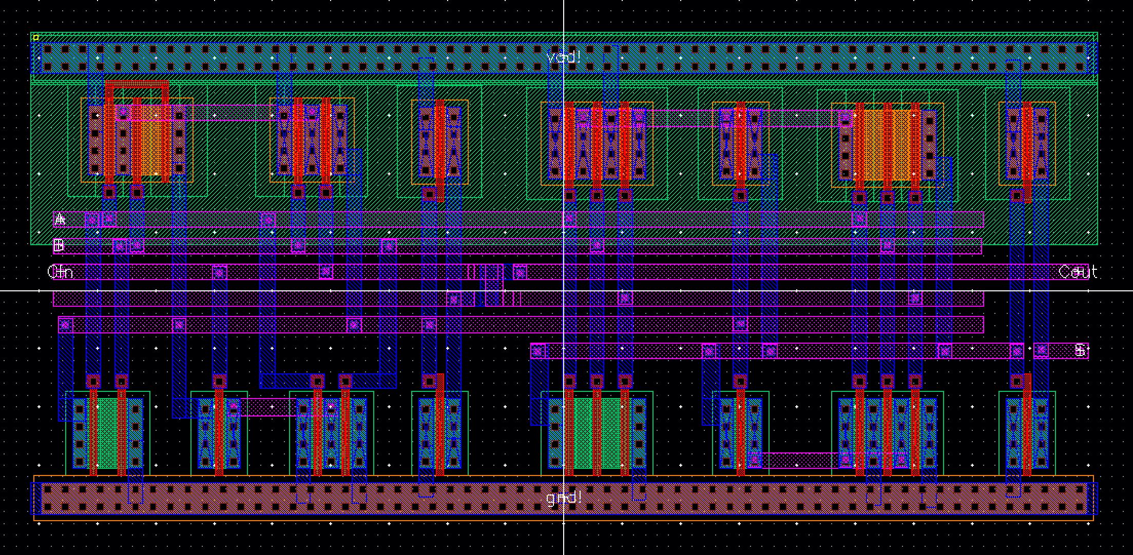
- A DRC check was then performed on the layout followed by a LVS to ensure that it matched the schematic.


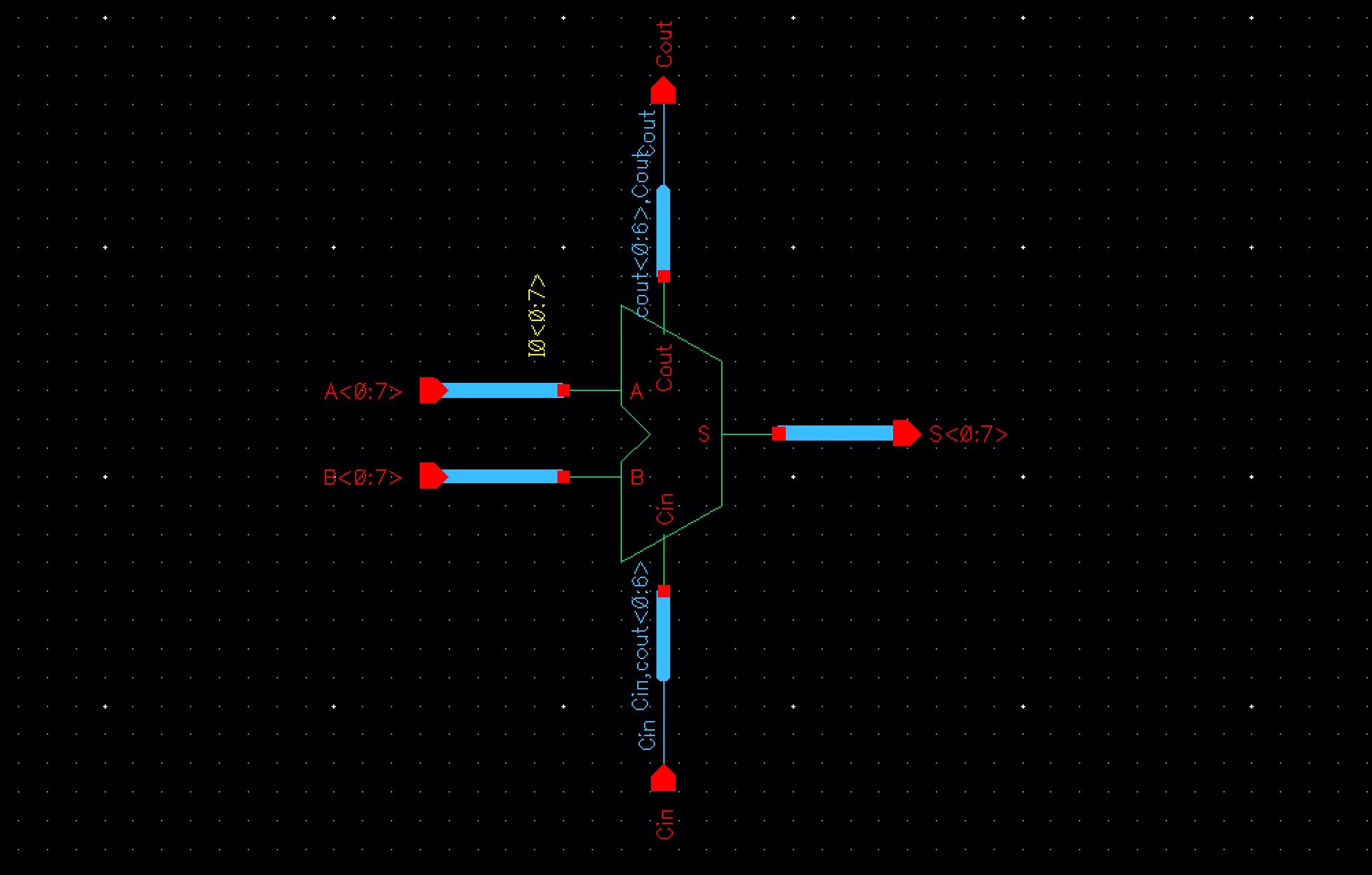
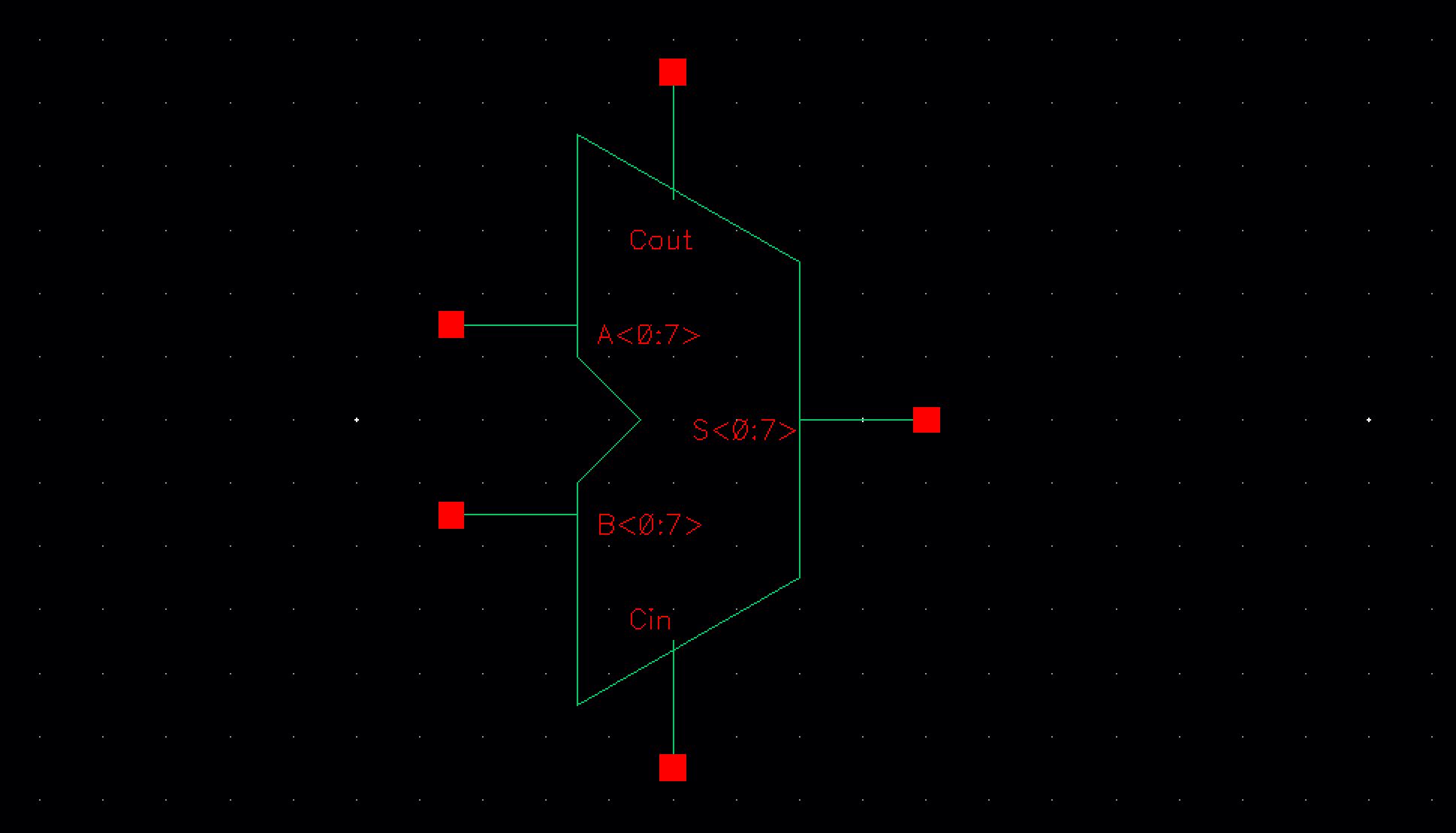
- The symbol created for the 1-bit full adder was then used to create the schematic for an 8-bit full adder.
- A symbol was also craetd for the 8-bit full adder.
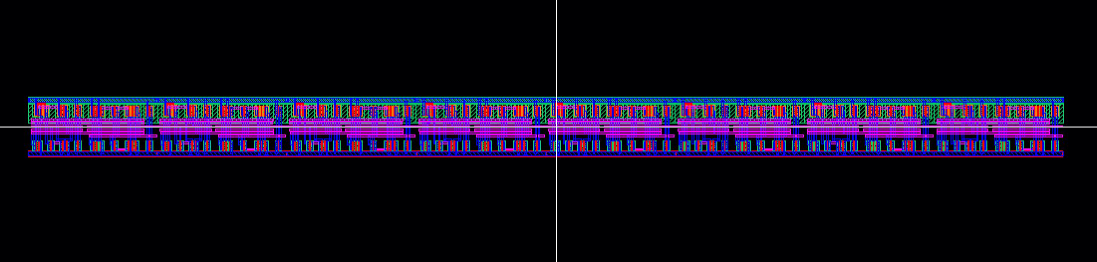
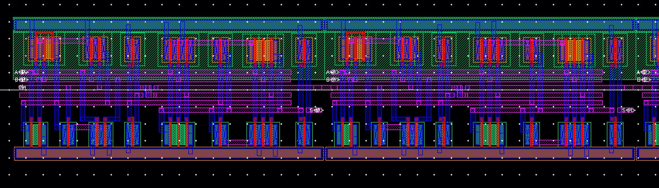
- A layout was then made for the 8-bit full adder by using the layout we had created for the 1-bit full adder.
- A DRC check was then performed on the layout with no errors found
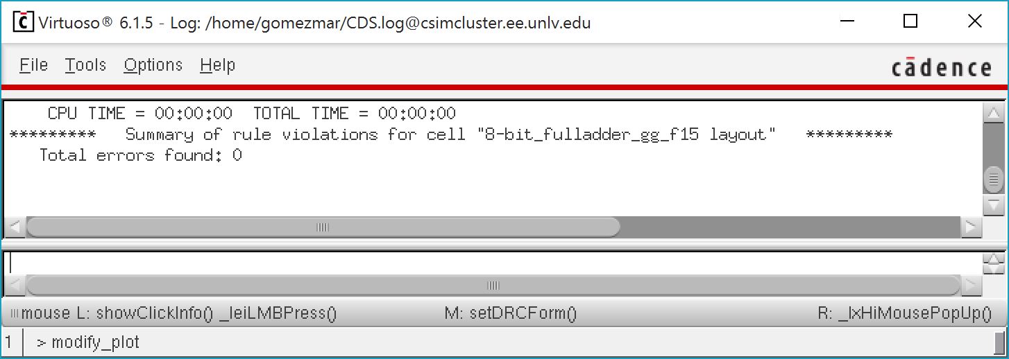
- An LVS was then done between the layout and schematic and the net-lists were found to match.

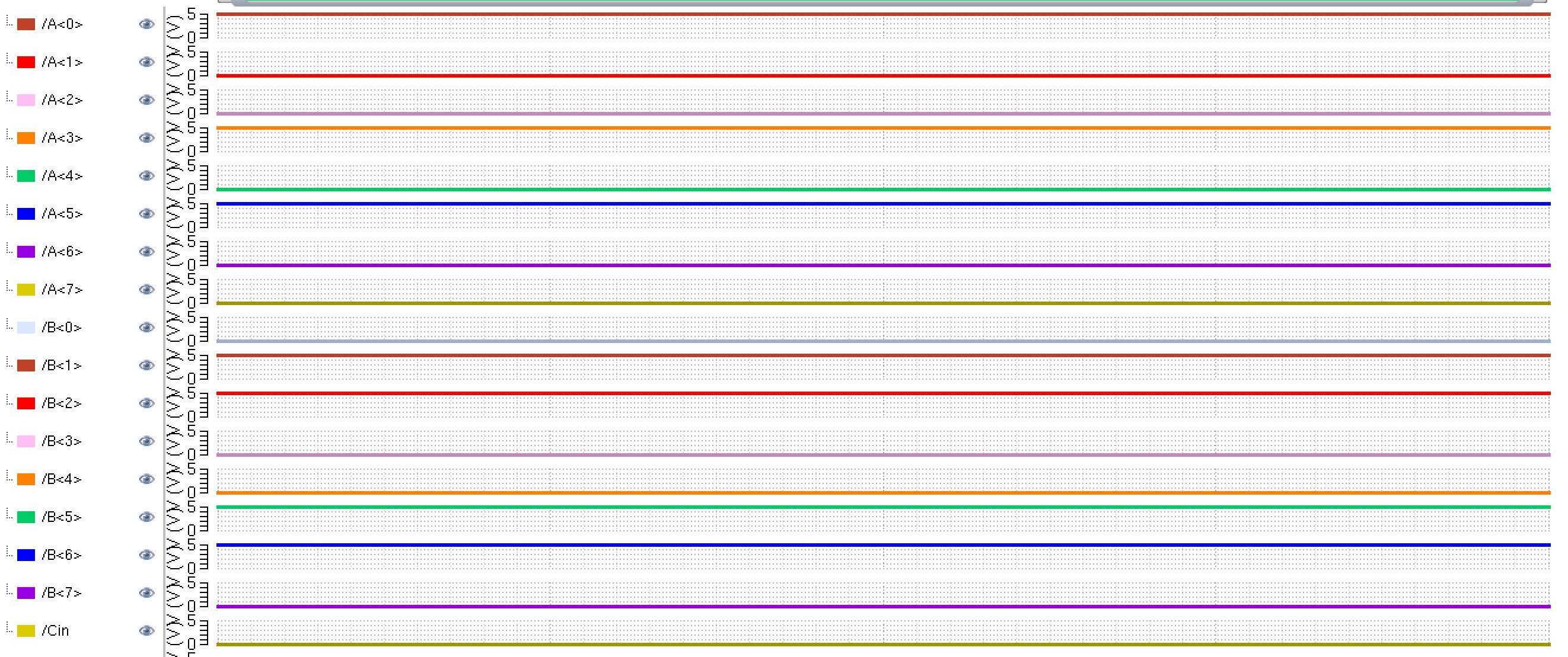
- The operation of the 8-bit Full Adder was then checked using a simulation.
- Some of the inputs on A and B were randomly set high in order to simulate a number.

- Our inputs can be seen bellow.
- The input on A is 00101001 which is equal to 41 decimal.
- The input on B is 01100110 which is equal to 102 decimal.
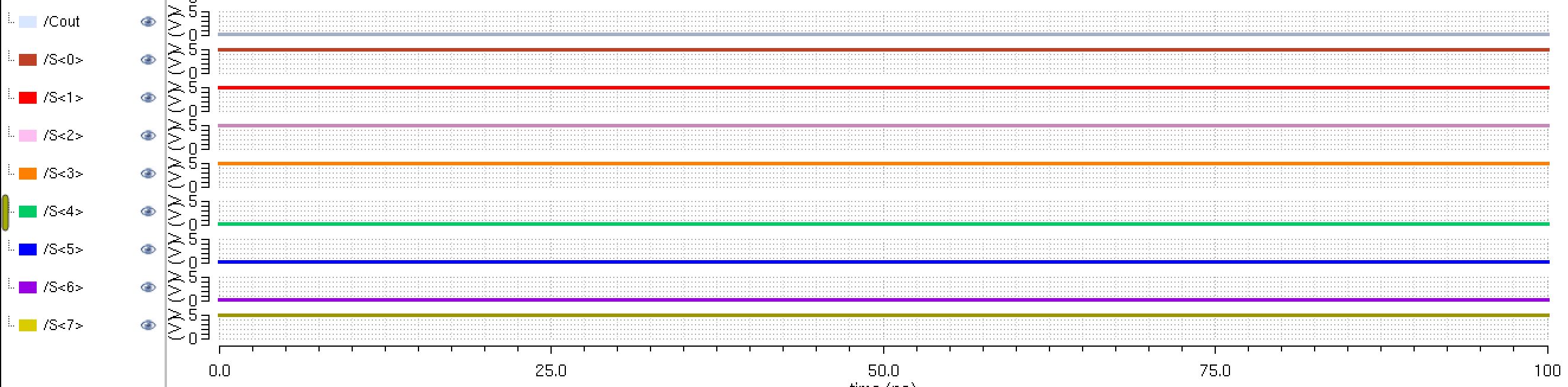
- Our outputs can be seen below.
- The output on S is 10001111 which is equal to 143 decimal which is 41+102 therefor our Adder works as expected.
- All of the files for this lab can be found here: lab7.zip