Lab description
The purpose of this lab was to layout and simulate a full adder.
Pre lab
- Back-up all of your work from the lab and the course.
- Go through Cadence Tutorial 4 seen here.
- Read through the lab in its entirety before starting to work on it
Lab Report
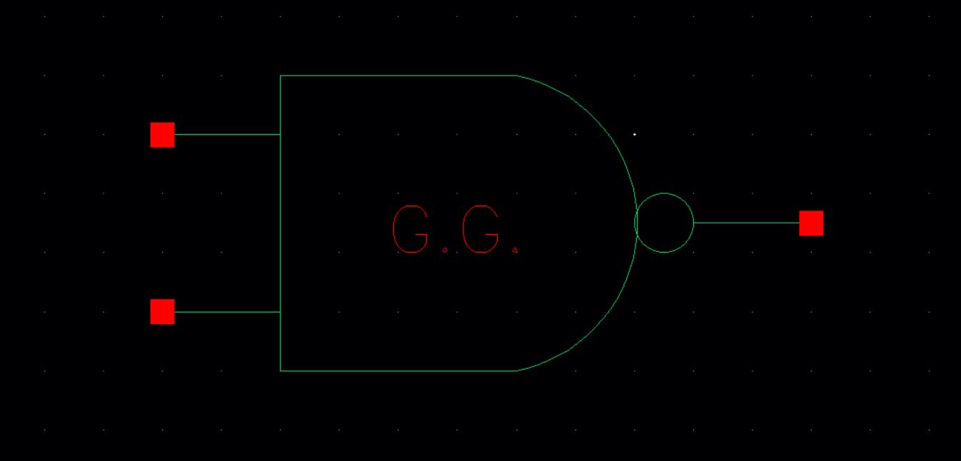
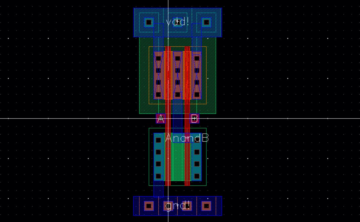
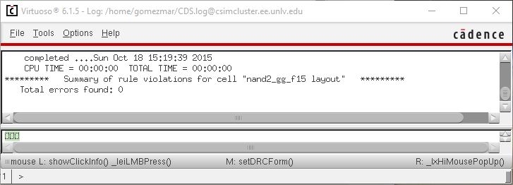
NAND gate
- A schematic was created for the NAND gate.
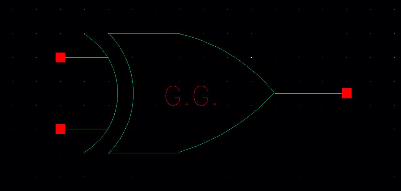
- Then a symbol was created from this schematic that looks like the symbol usually used for this gate.
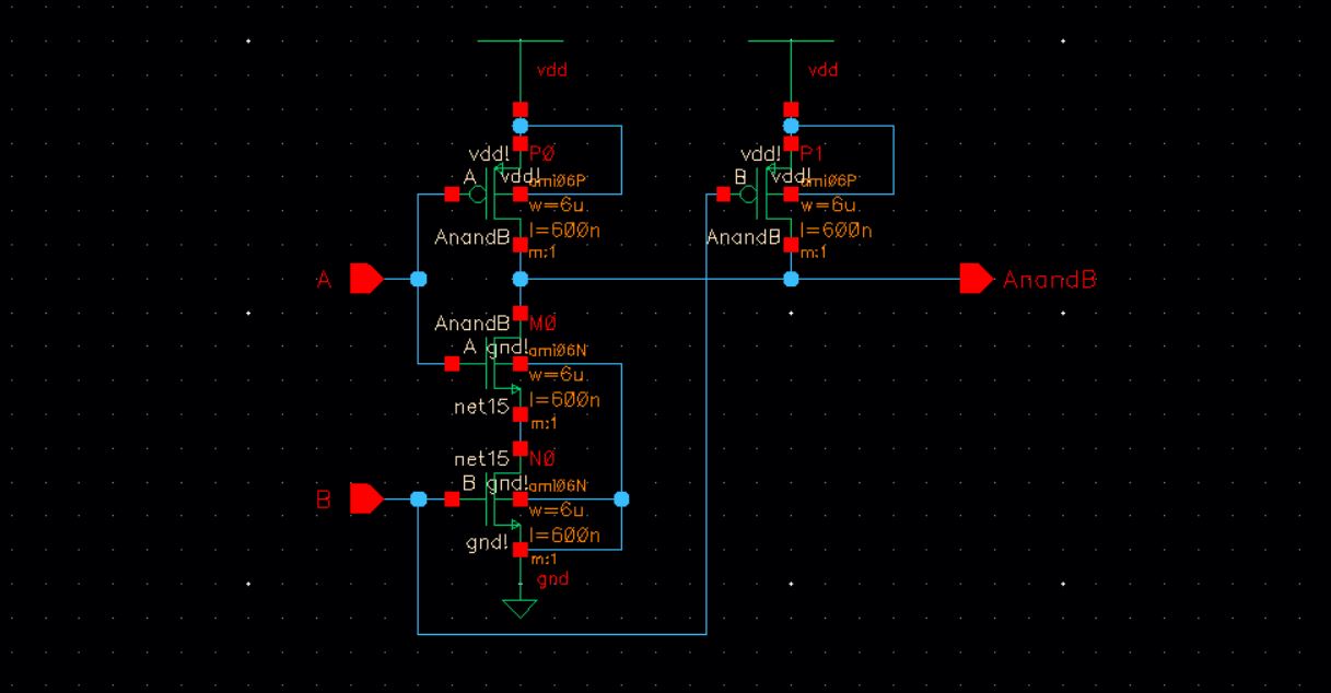
- Then a layout was created from the schematic, using standard cell frames.
- A DRC check was performed on the layout to ensure there were no errors.
- An LVS was performed between the extracted layout and the schematic, the net-lists matched.

XOR gate
- A schematic was created for the XOR gate.
- Then a symbol was created from this schematic that looks like the symbol usually used for this gate.
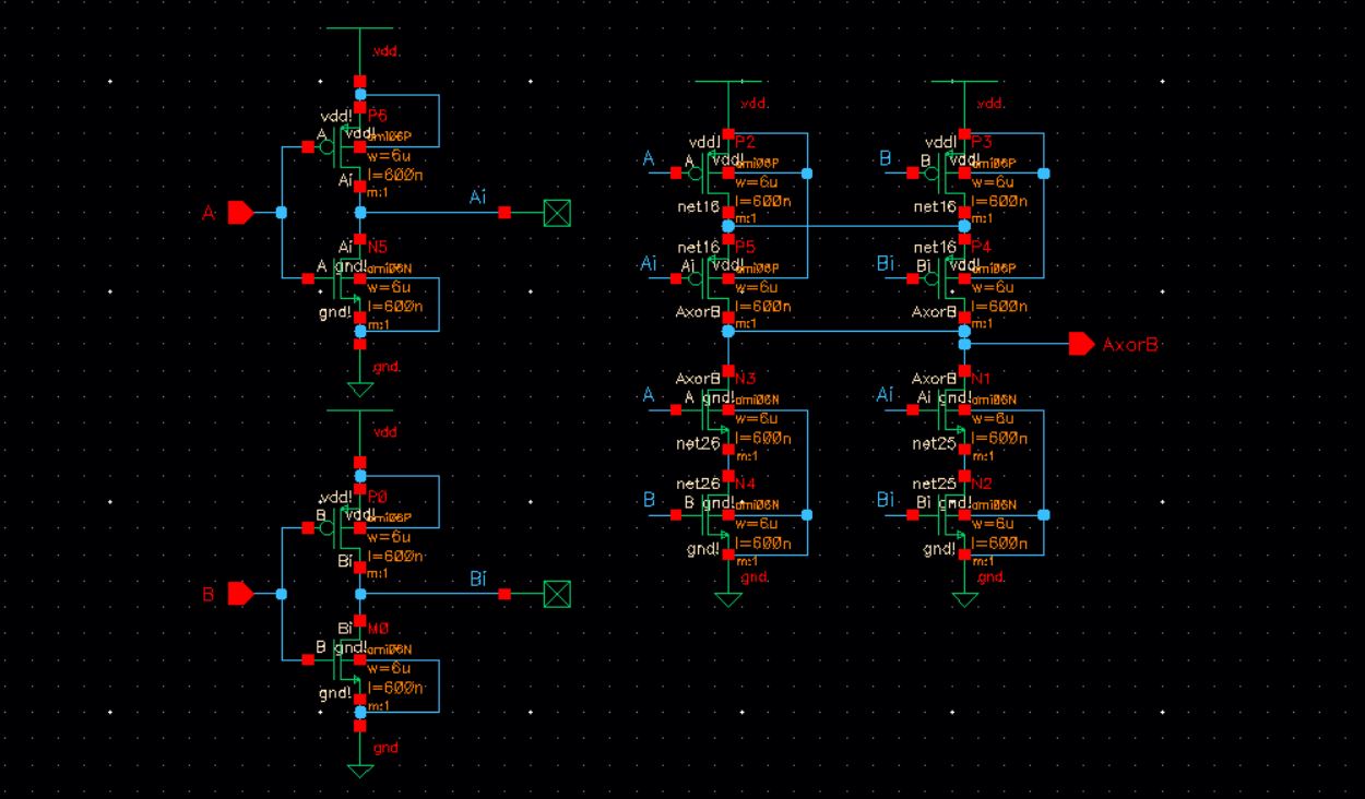
- Then a layout was created from the schematic, using standard cell frames.
- A DRC check was performed on the layout to ensure there were no errors.
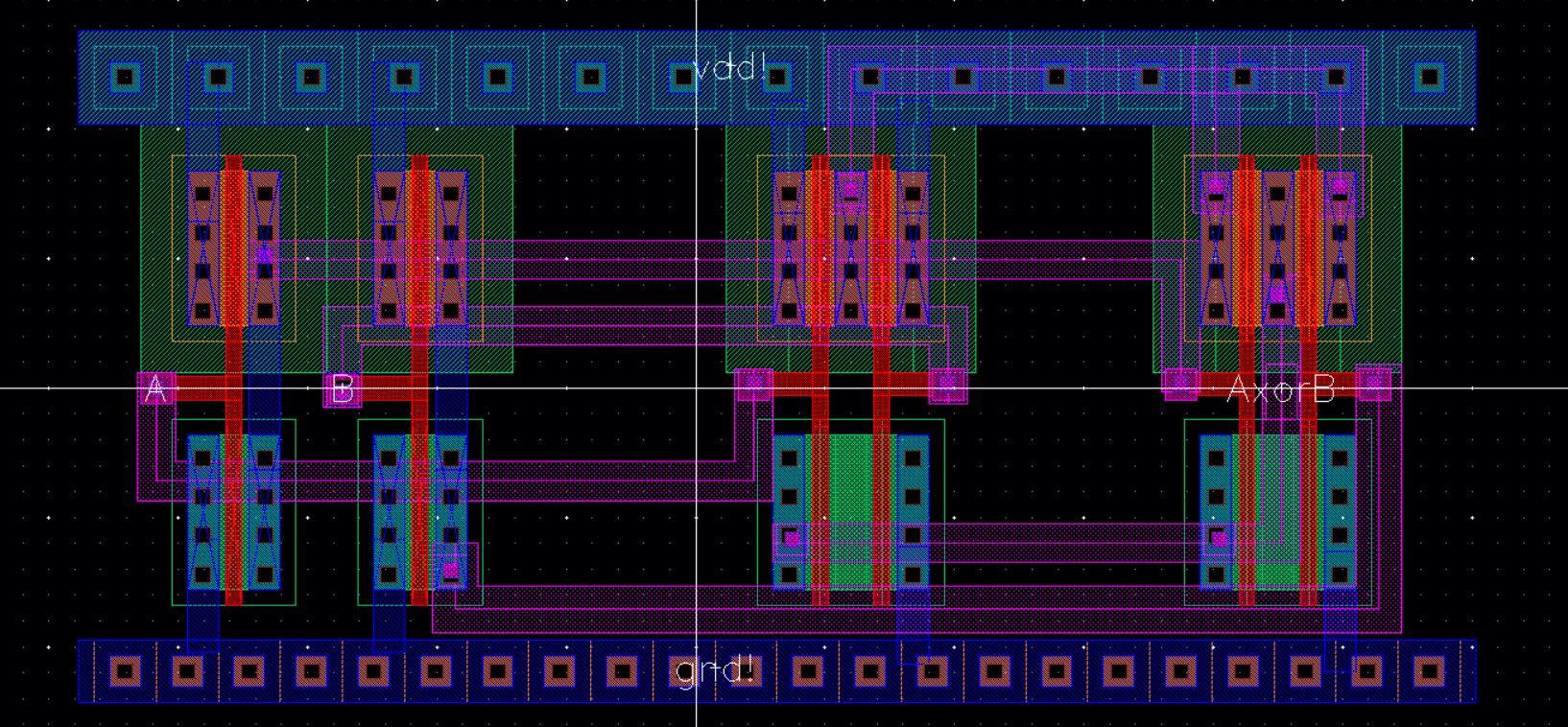

- An LVS was performed between the extracted layout and the schematic, the net-lists matched.

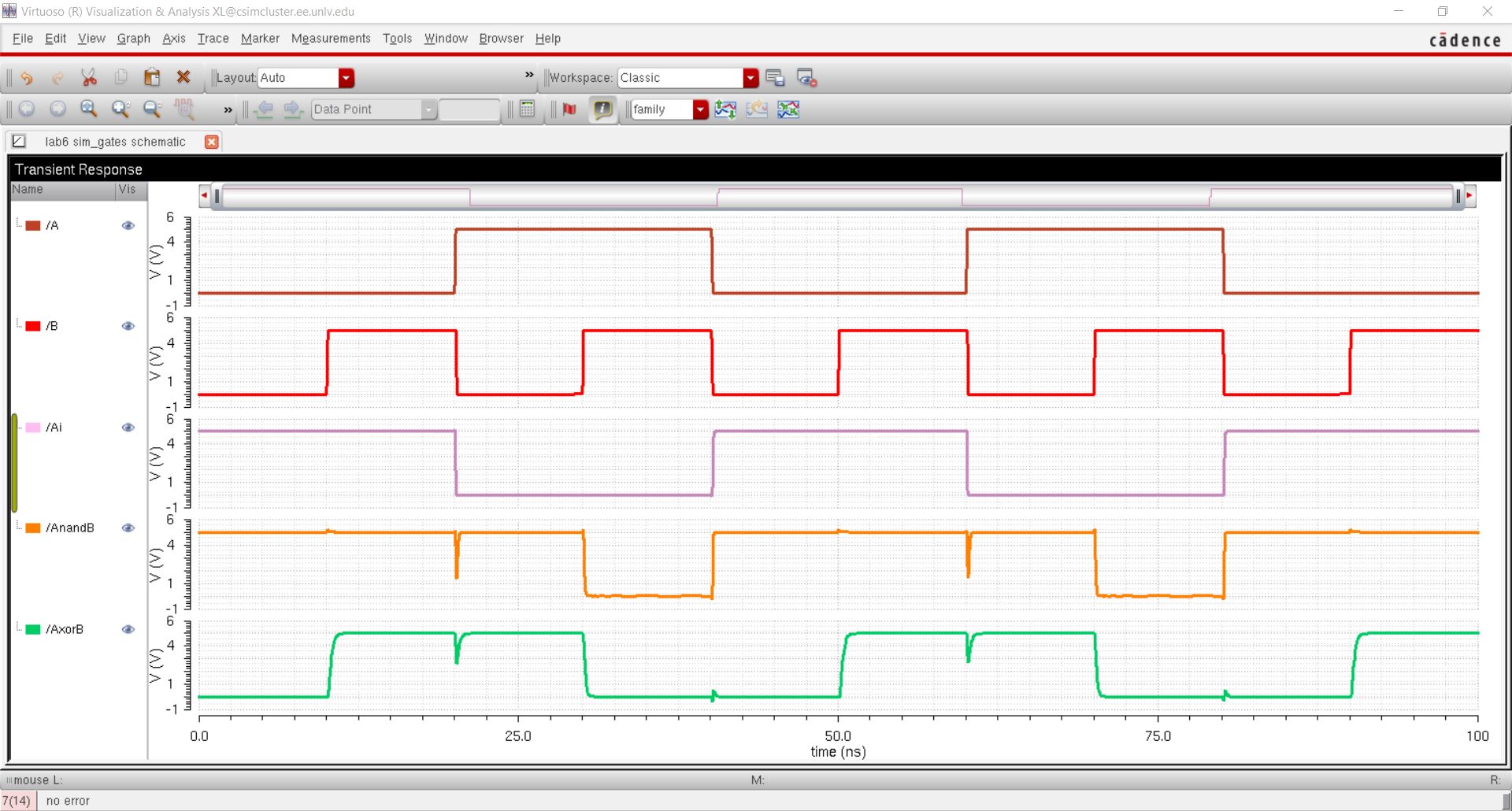
- A schematic for simulation was then created to test the gates.
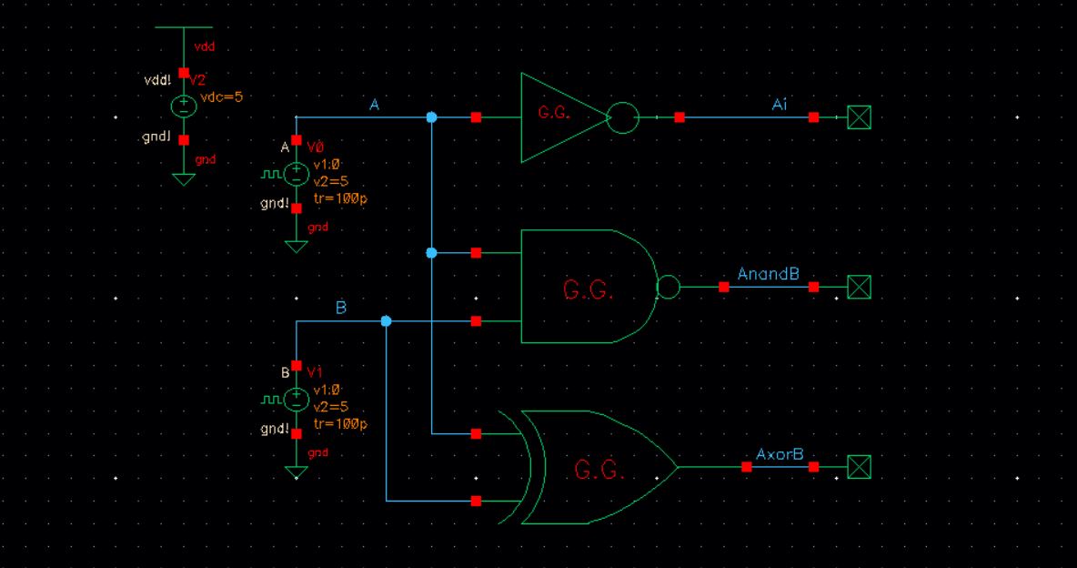
- The results obtained were what is expected from these gates.
- A truth table for the expected results can be seen below.
| A | B | A' | AnandB | AxorB |
| 0 | 0 | 1 | 1 | 0 |
| 0 | 1 | 1 | 1 | 1 |
| 1 | 0 | 0 | 1 | 1 |
| 1 | 1 | 0 | 0 | 0 |
Full adder
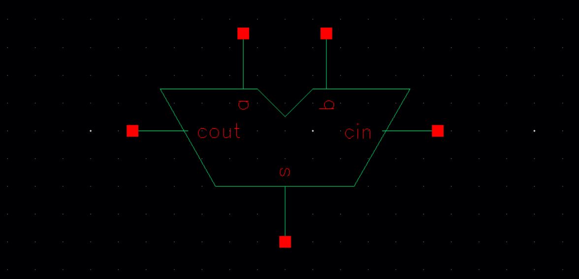
- A schematic was created for a full adder.
- Then a symbol was created from this schematic that looks like the symbol usually used for this component.

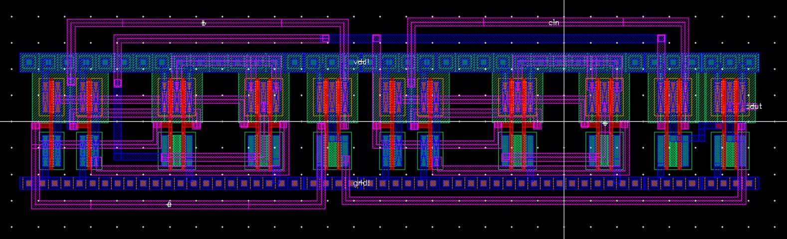
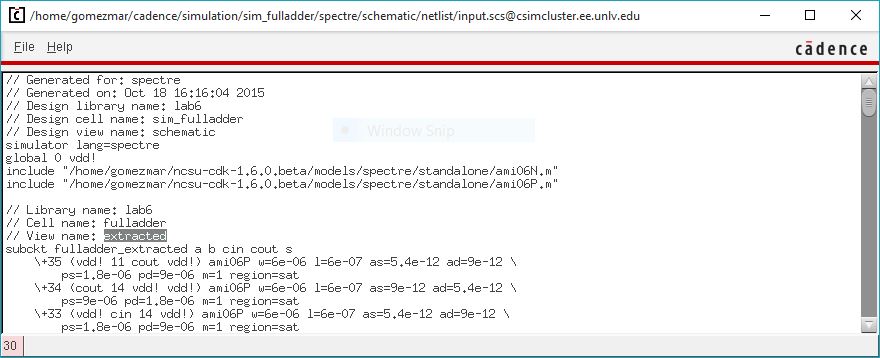
- Then a layout was created from the schematic, using the layouts previously created which use standard cell frames.
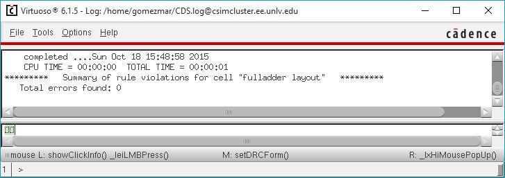
- A DRC check was performed on the layout to ensure there were no errors.
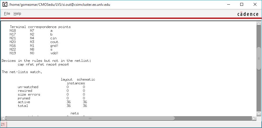
- An LVS was performed between the extracted layout and the schematic, the net-lists matched.
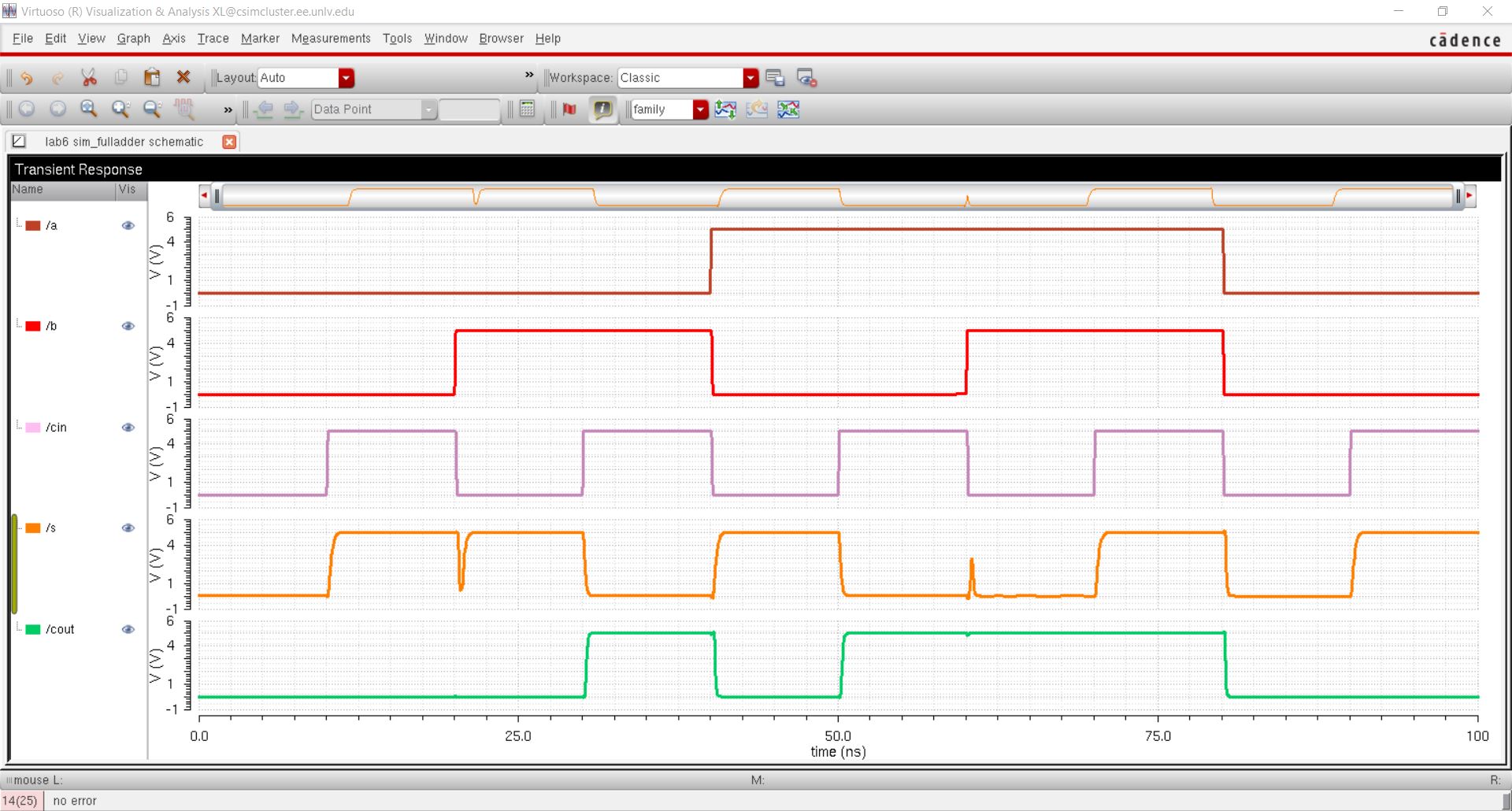
- A schematic was then created to test the full adder.

- The results obtained were what is expected from these gates.
- A truth table for the expected results can be seen below.
| a | b | cin | s | cout |
| 0 | 0 | 0 | 0 | 0 |
| 0 | 0 | 1 | 1 | 0 |
| 0 | 1 | 0 | 1 | 0 |
| 0 | 1 | 1 | 0 | 1 |
| 1 | 0 | 0 | 1 | 0 |
| 1 | 0 | 1 | 0 | 1 |
| 1 | 1 | 0 | 0 | 1 |
| 1 | 1 | 1 | 1 | 1 |
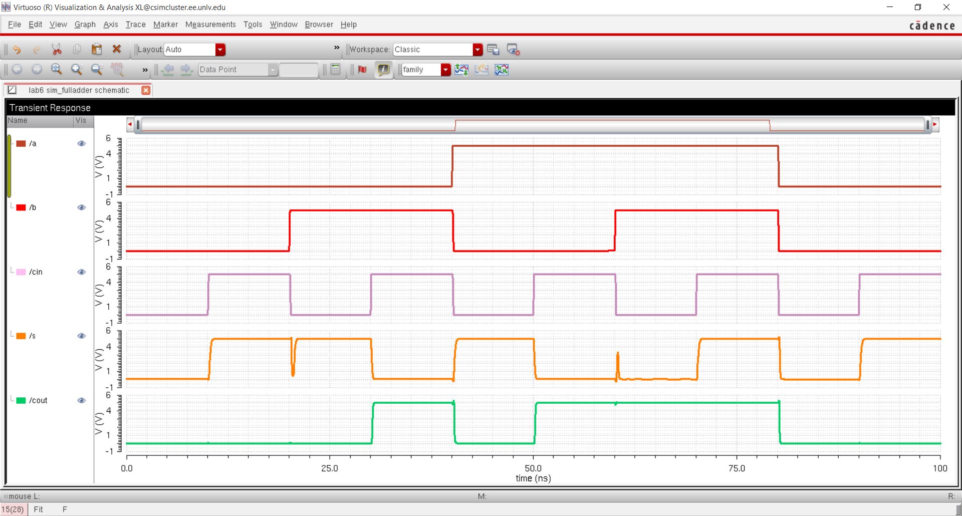
- The same simulation was then perfomed using the extracted layout instead of the schematic.
- The results obtained were similar to the simulation using the schematic.
- All of the files for this lab can be found here: lab6.zip