Lab description
The purpose of this lab was to layout a 10-bit DAC.
Lab Report
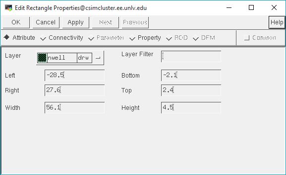
- The layout for a 10K resistor using the n-well layer was completed.
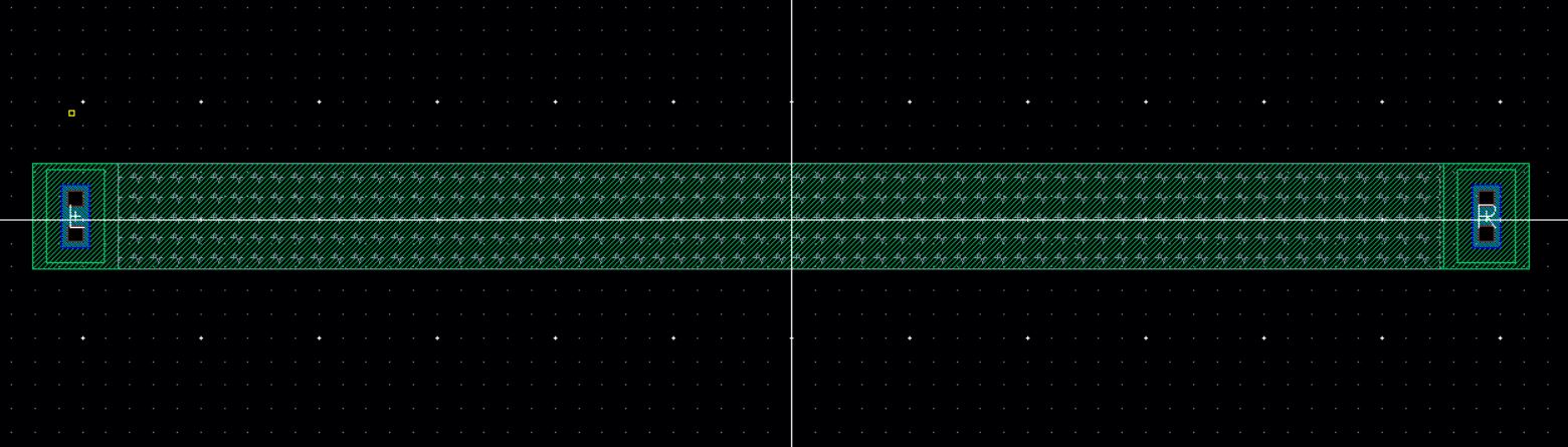
- In order to determine the size of the n-well square the MOSIS process rules were considered.
- The minimum width for the n-well is 12 lambda, which is 3.6um since lambda is 300nm.
- A width sligtly larger than 3.6um, 4.5um, was used here.
- For the process used here, C5 process, the sheet resistance is about 800 ohms per square
- To determine the length the following formula was used:
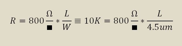
- Solving for L we get:
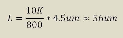
- For this process the grid distance is 0.15um so a length of 56um will fall outside the grid since it's not divisible by 0.15um.
- Therefor the length is increased slightly to 56.1um which is divisible by 0.15um.
- Checking our extracted layout we see the resistance obtained is 10.18K which is really close to 10K.

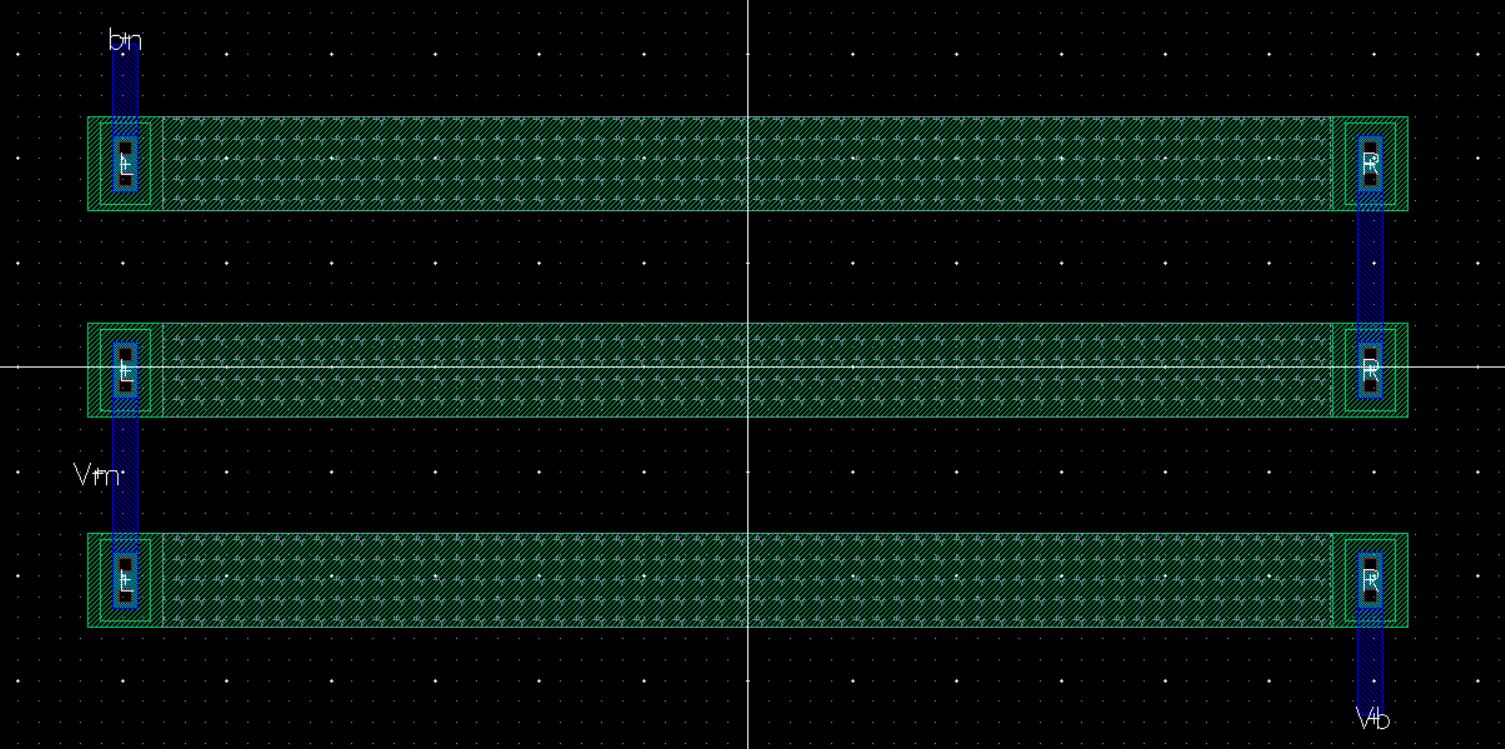
- Using the layout for the 10K ressitor created before, the layout for a section of the DAC was created, by using two resistor in series to create 2R.
- A DRC check was performed on the layout to make sure there were no errors.
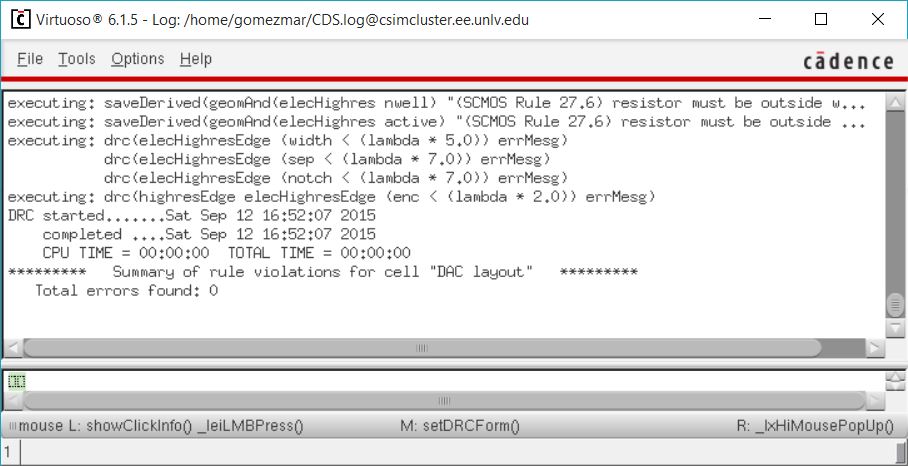
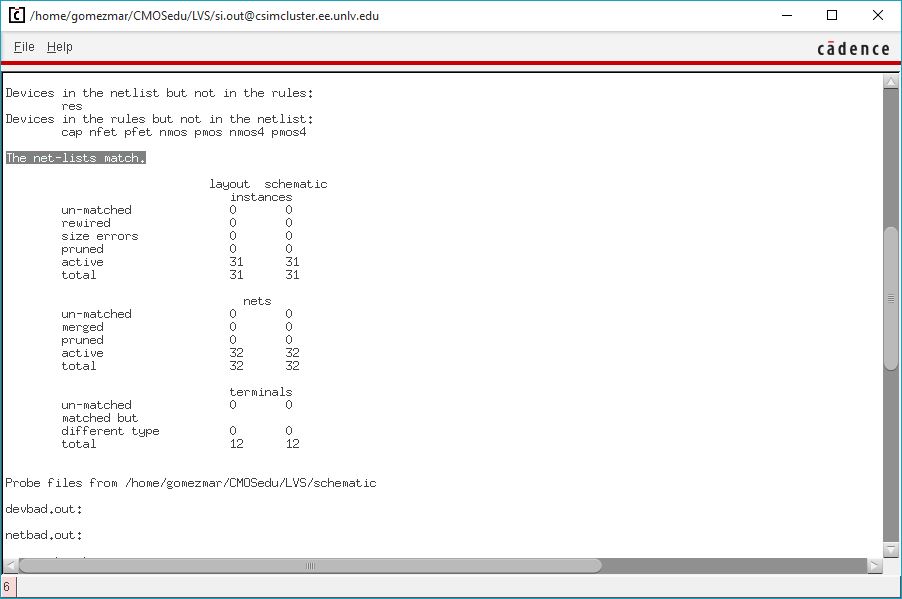
- The layout was then LVS to make sure it matches the schematic created on Lab 2.

- The same process was performed with the bottom section of the DAC which containes two 2Rs.

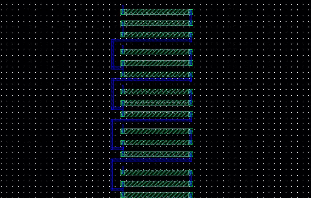
- The layouts created for the sections were then used to create the layout for the 10-bit DAC by instanciating 10 of them.
- A DRC check was done to make sure there were no errors in the layout.
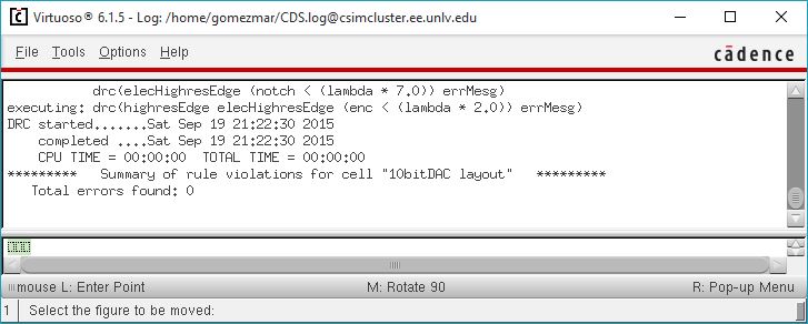
- An LVS was the performed and the layout was found to match the schematic for the 10-bit DAC.
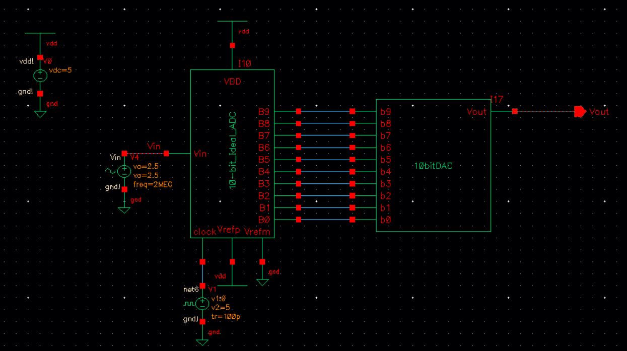
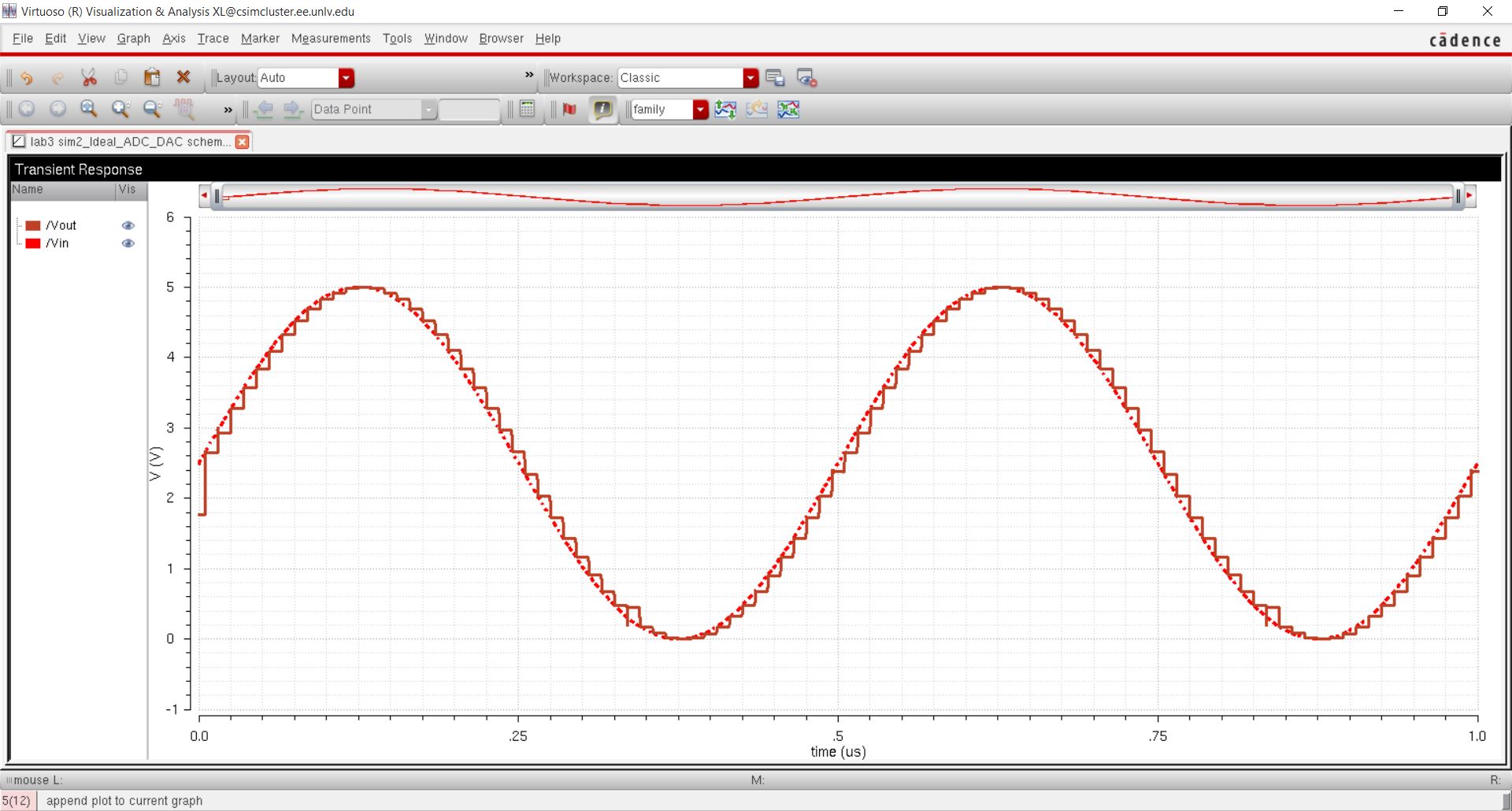
- The deisgn was then checked by simulating the entire design using the extracted layout for simulation.
- The results obtained are what was expected.
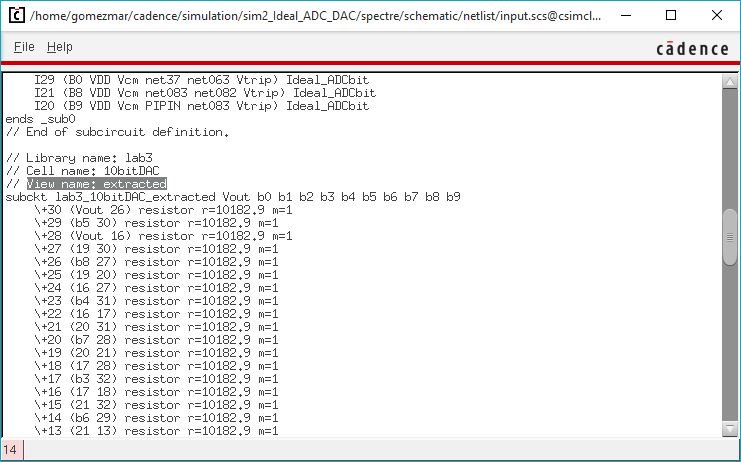
- The netlist was checked to ensure the extracted layotu was used for the simulation.
- All of the files for this lab can be found here: lab3.zip