Lab description
The purpose of this lab was to implement a 10-bit DAC.
Prelab
- The zip file with the components for this lab was added to the design directory and unzipped.
- From there the Ideal ADC DAC schematic was opened.
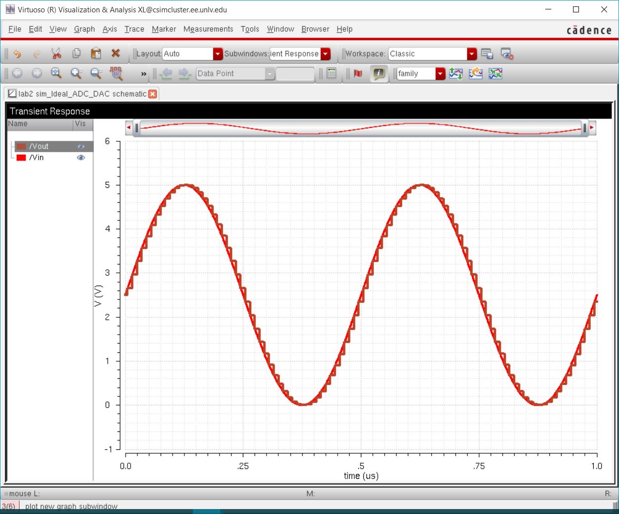
- The simulation was then ran.
- In order to change the properties of the plot the name of the trace was right clicked and trace properties was selected.
- This opens the trace properties window where the line tickness and type of line can be modified.
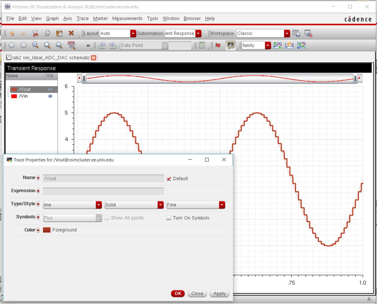
- The lines were changed to a solid line and the thickness was adjusted in order for the plot to be easier to see.
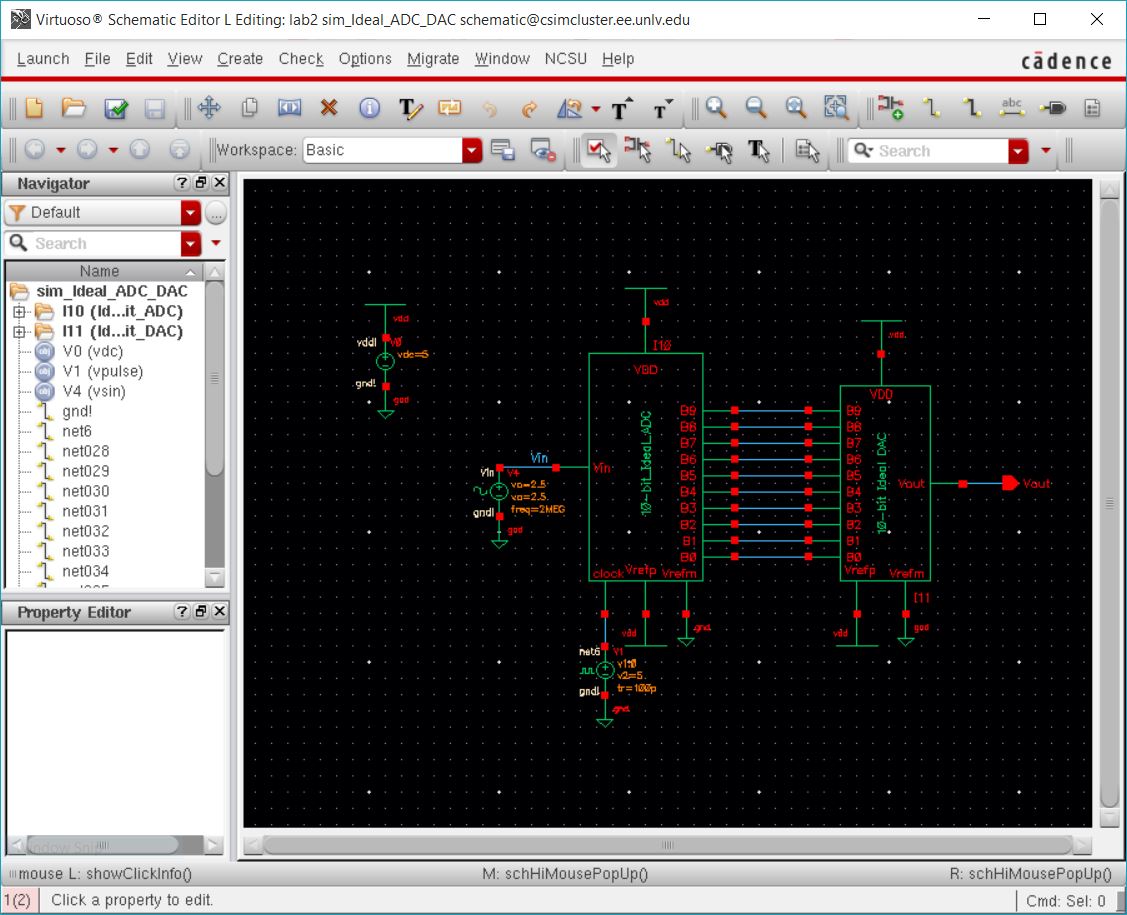
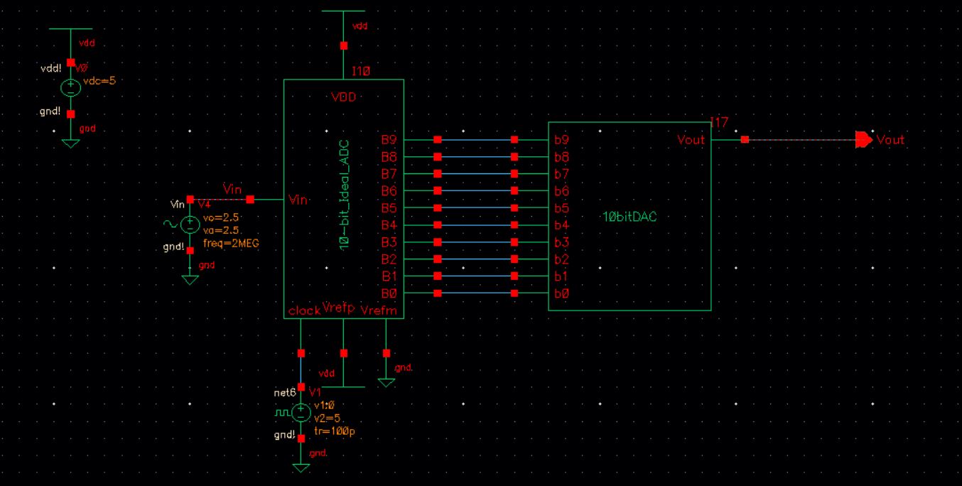
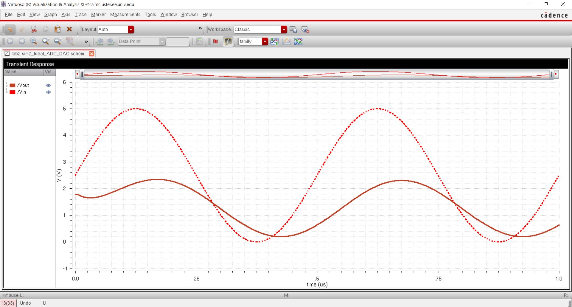
- The design consists of an ADC and a DAC. An analog signal such a sine wave is fed into the input of the ADC.
- This produces 10 different outputs B[9:0], this outputs represent a 10-bit binary number.
- This digital output is then fed into the DAC which inputs the digital output and output an analog signal. By changing the parameter of the original analog signal we are able to see how the output always stays close to the original signal.

-
The Least Significant Bit of the Digital output is determined by:
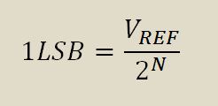
where VREF is the maximum possible value that can be represented and N is the number of bits used to represent the digital output. -
In this case the number of bits being used is 10, and the reference voltage, VREF, is 5v. Plugging in these values we get:
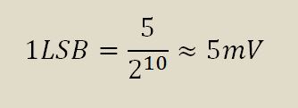
- Thus a change of about 5mV will produce a change on the digital output of the ADC.
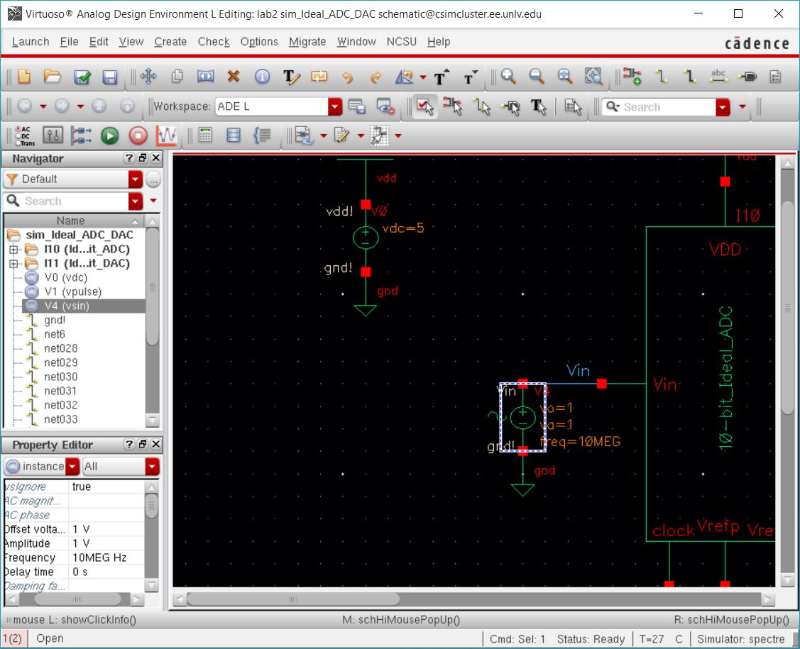
- This can be seen by changing the input signal's amplitude to a small value, such as 10mV in this example.
- Here it can be seen that for about each 5mV chnage in the input there is a chnage in the output.

Lab Report
- The design for our DAC was based on the schematic seen bellow.
- To start I made an schematic for each of the sections of the DAC exept the last one since all of them are identical.
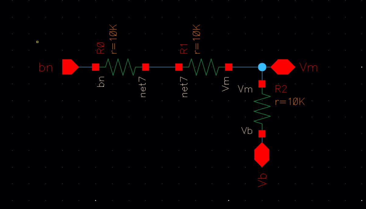
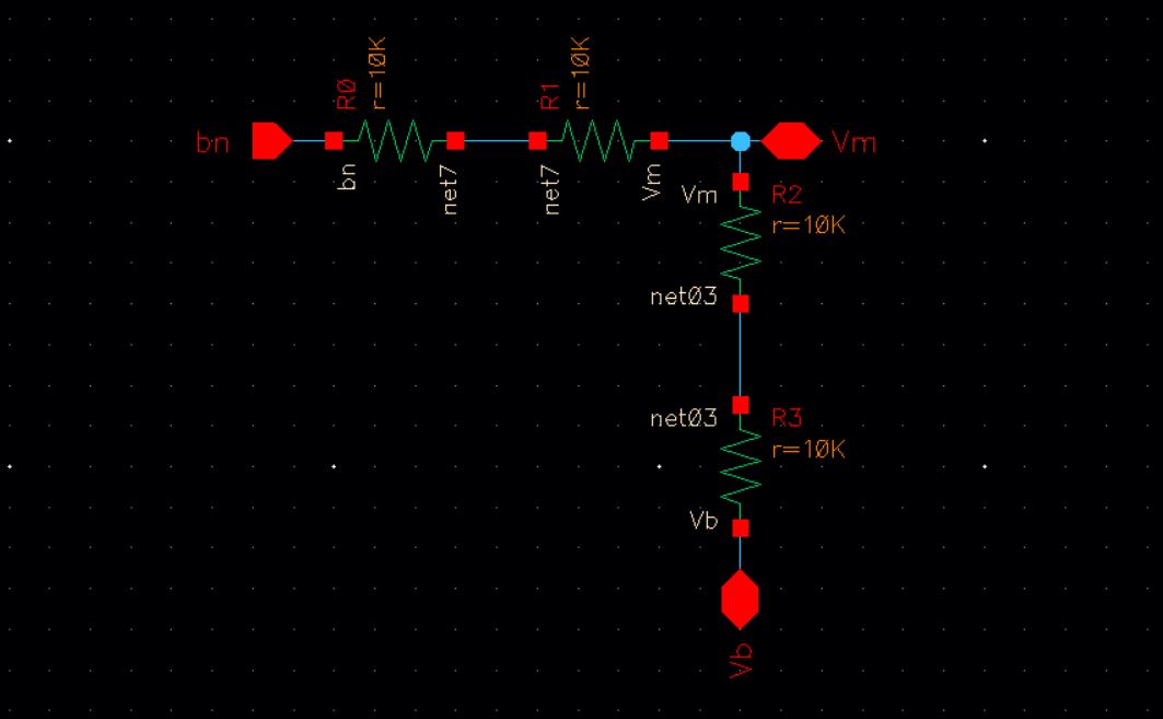
- Then I created a symbol for the previously seen schematic.
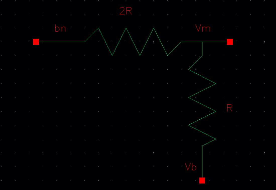
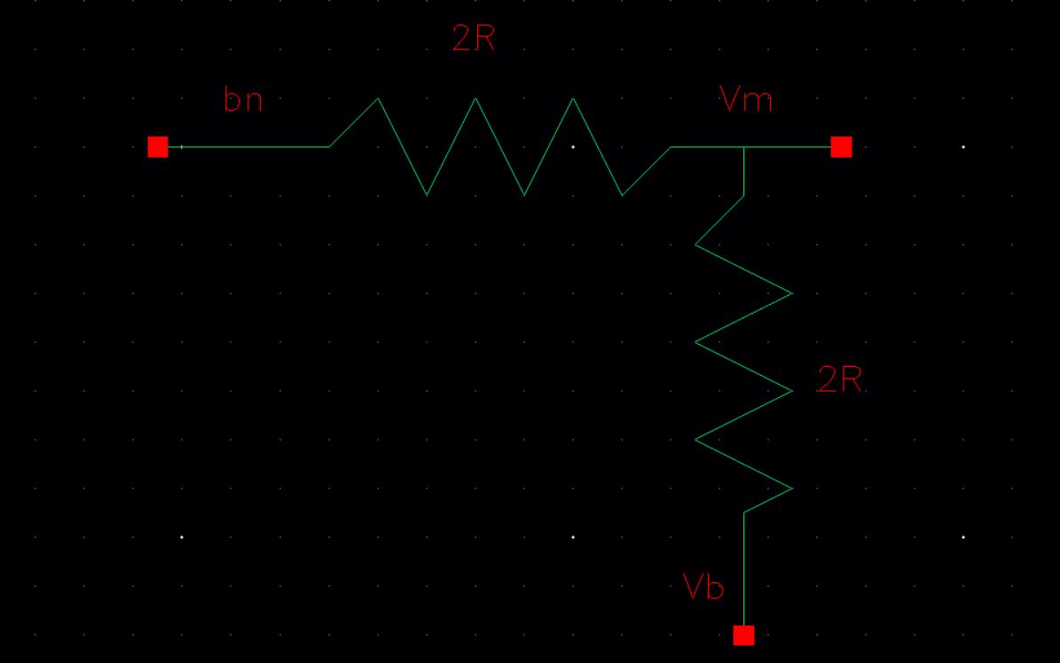
- Then I repeated the same progress to make a schematic and symbol for the bottom section of the DAC.
- Then I create a new schematic for our 10-bit DAC.
- I created instances of the previously created symbols and wired them together to create the 10-bit DAC
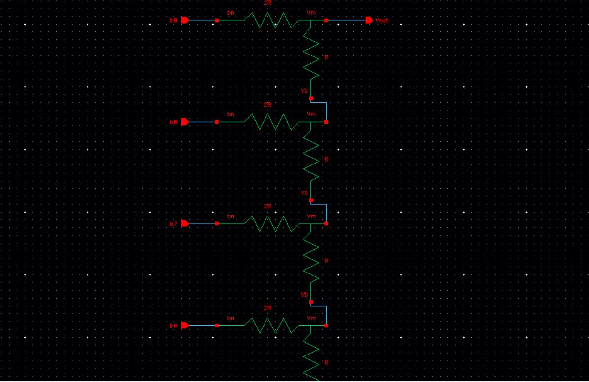
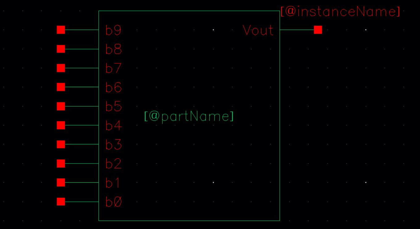
- Then I create a symbold from the 10-bit DAC schematic
- This symbol can be used in place of the previously used Ideal_10-bit_DAC.
- The output resistance of this design was then calculated.
- This was calculated by grounding all the inputs to the DAC and following the process seen below.

- The delay to the circuit was then calculated.
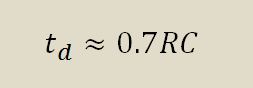
- The output resistance was found to be equal to R.
- This calculation was used to find the delay the DAC has driving a 10 pF load.
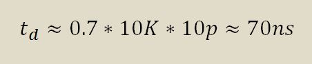
- The calculated delay value was then checked using simulations
- In order to do this, all the outputs of the DAC were grounded except for b9.
- A pulse source with an amplitude of 1V was connected to b9, and a 1pF load was added.
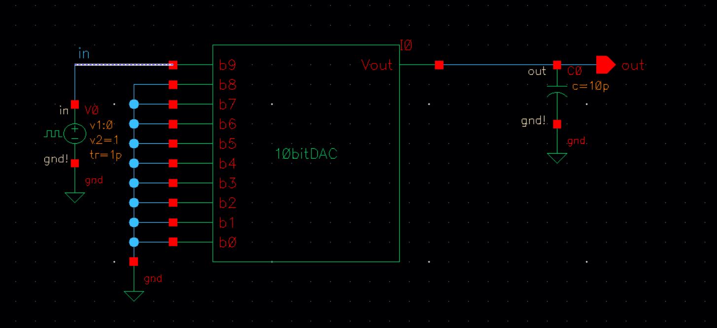
- The resulting simulation confirms the previously computed calculations.
- At 70ns the output is at 50% of its max value.

- Then the current DAC in the sim_Ideal_ADC_DAC schematic was replaced with the DAC I created.
- When the design was simulated a convergence problem was found.
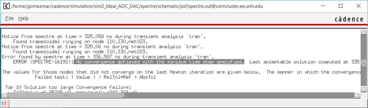
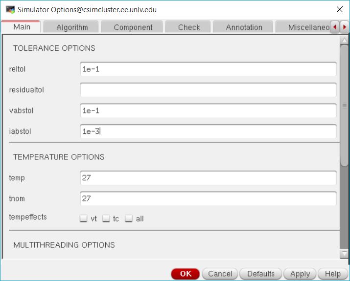
- The convergence problem was fixed by changing the simulator options as shown below.
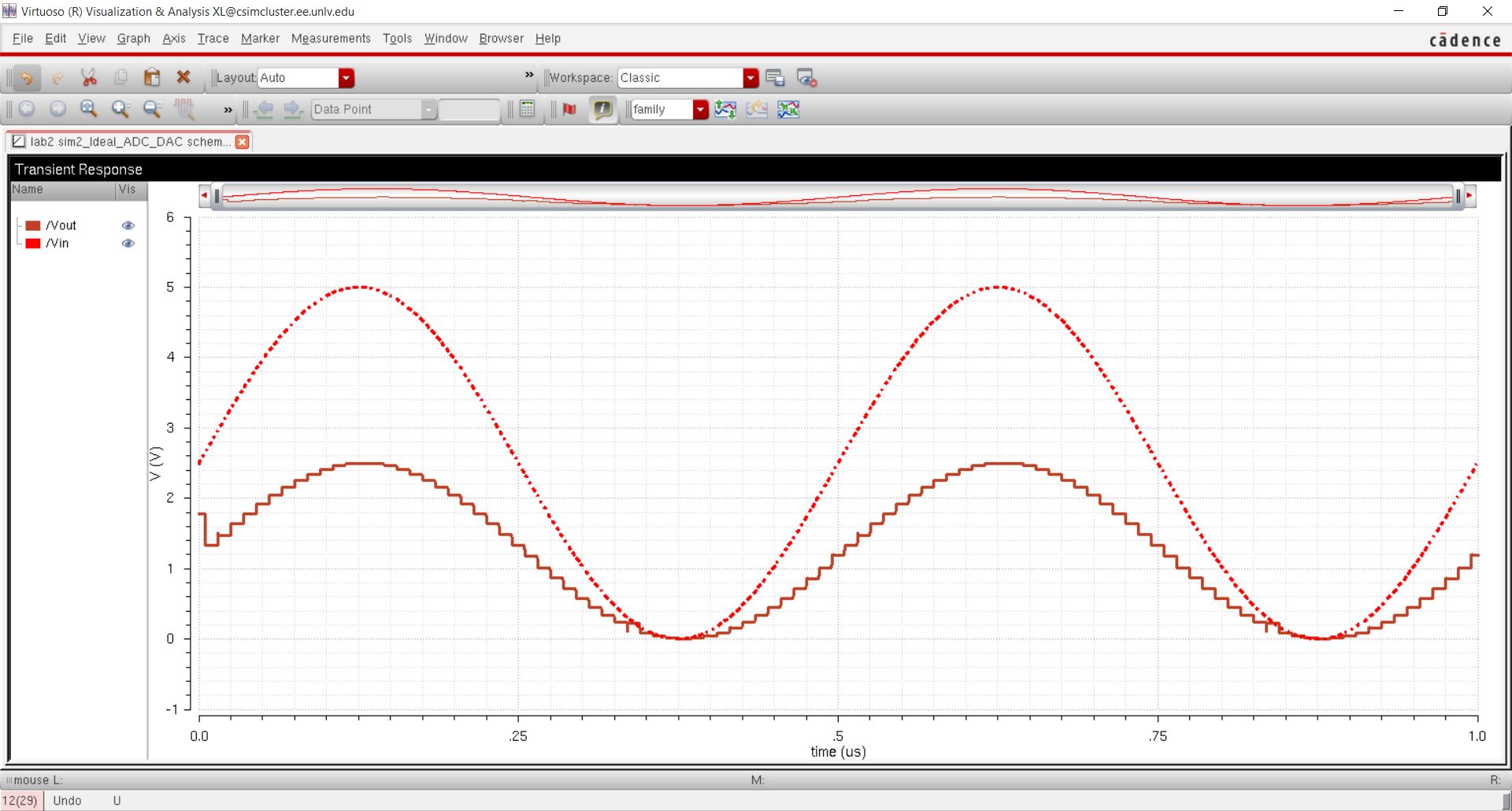
- The design was simulated to check its opertation.
- The resulting output was what's expected, a waveform that closely follows the original sine wave input to the ADC.

- Different loads were then added to the design to test how they would affect the output.
- With a 10K load, the output was cut in half from its original amplitude.
- This is due to the output resistance of the DAC which is R, 10K in this case, which is equal to the load. This creates a voltage divider and since they both have the same resitance the resulting output is one half the input.
- With a 10pF load added to the 10K load the output is seen below.
- And with just a 10pF load added the output is a delayed version of the input with a smaller amplitude.
