Lab 6 - ECE 421L
Degracia, Manuel C.
degracia@unlv.nevada.edu
19 October 2015
Pre-Lab
- Go through Tutorial #4.
- Back-up all work from the lab and the course.
Post-Lab
Objectives:
- Draft
the schematics of a 2-input NAND gate (Fig. 12.1), and a 2-input XOR
gate (Fig. 12.18) using 6u/0.6u MOSFETs (both NMOS and PMOS)
- Create layout and symbol views for these gates showing that the cells DRC and LVS without errors
- ensure
that your symbol views are the commonly used symbols (not boxes!) for
these gates with your initials in the middle of the symbol
- ensure all layouts in this lab use standard cell frames that snap together end-to-end for routing vdd! and gnd!
- use a standard cell height taller than you need for these gates so that it can be used for more complicated layouts in the future
- ensure gate inputs, outputs, vdd!, and gnd! are all routed on metal1
- Use cell names that include your initials and the current year/semester, e.g. NAND_jb_f19 (if it were fall 2019)
- Using Spectre simulate the logical operation of the gates for all 4 possible inputs (00, 01, 10, and 11)
- comment on how timing of the input pulses can cause glitches in the output of a gate
- Your html lab report should detail each of these efforts.
- Using these gates, draft the schematic of the full adder seen below
- Create a symbol for this full-adder (example)
- Simulate, using Spectre, the operation of the full-adder using this symbol
- Layout the full-adder by placing the 5 gates end-to-end so that vdd! and gnd! are routed
- full-adder inputs and outputs can be on metal2 but not metal3
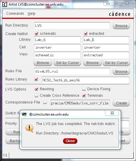
- DRC and LVS your full adder design.
Process:
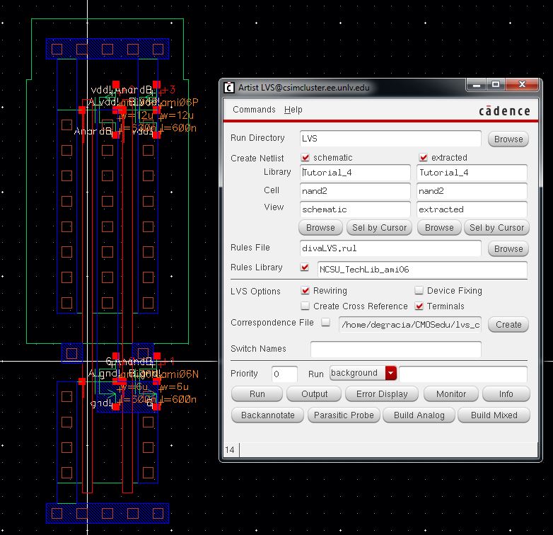
2-Input NAND Gate:
By following the steps in Tutorial #4, one can create the 2-Input NAND Gate displayed below.
Schematic: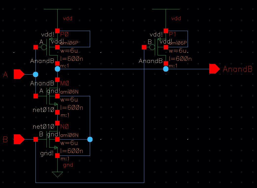
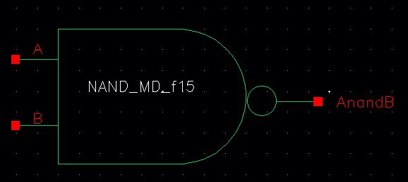
Symbol:
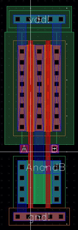
Layout:
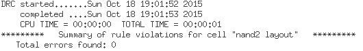
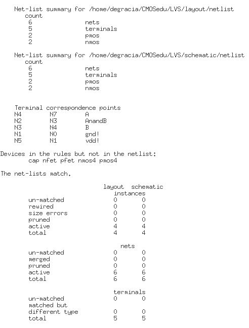
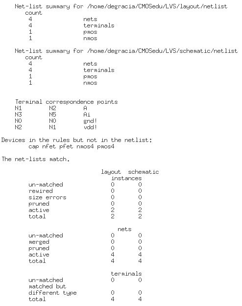
Extracted View/LVS:

Output:
2-Input XOR Gate:
Following
the same steps and concept of the NAND Gate explained in Tutorial #4,
create the schematic below for the XOR Gate. Be sure that all the
MOSFETS sizes are the approriate length and width for this may cause
errors later in the process.
Schematic: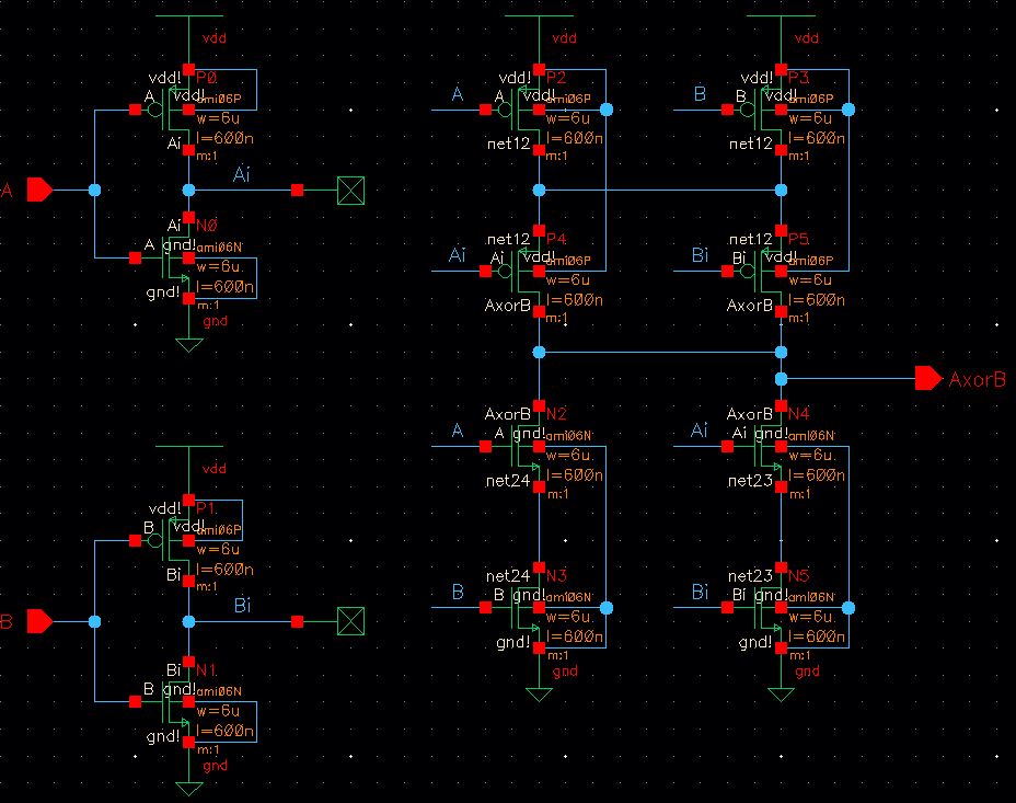
Symbol: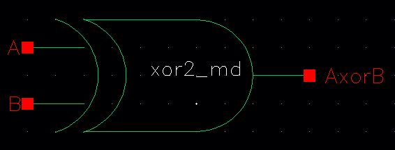
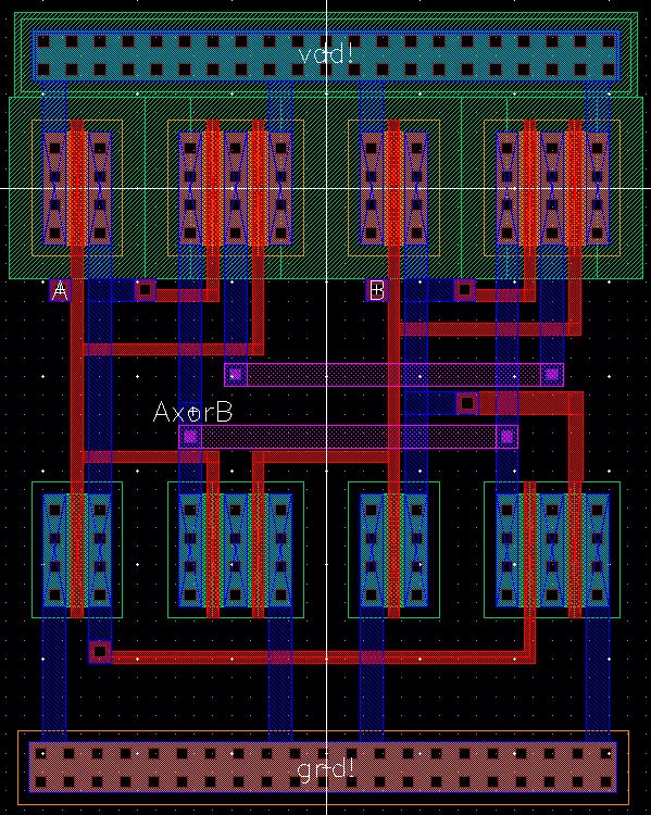
Layout:
Using
the schematic as reference, create the following layout.
In order to not have paths crossing each other (such as poly and metal1
layers connecting at intersections where they shouldn't), use metal2
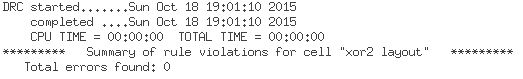
and m2_m1/m1_poly combinations to get the needed connections. DRC and
LVS.
Extracted:
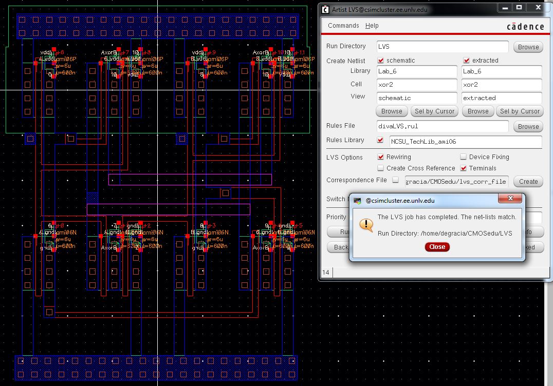
Output: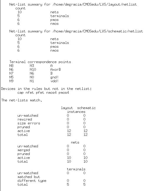
Simulation of Inverter, XOR, NANDTo test the validity of the created gates, we can create a simulation cell.
Schematic:
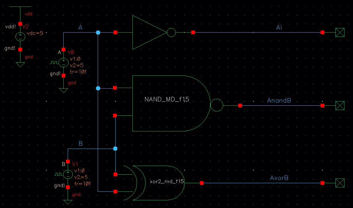
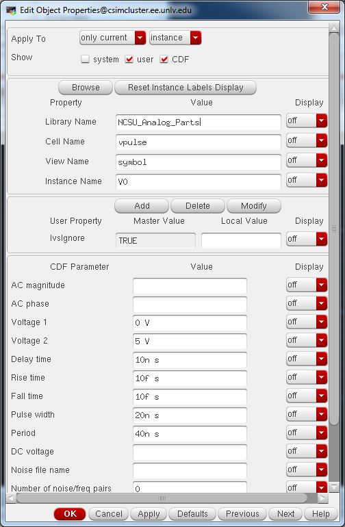
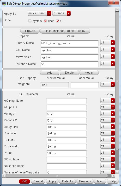
Use the following voltage parameters for the inputs (variation permitted).
Analysis: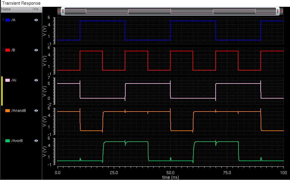
Truth Tables:
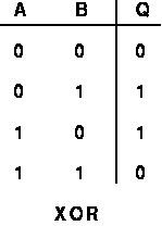
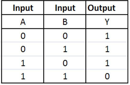
Comparing
the truth tables and transient response, one can see that the created
gates work properly. Noise found in the transient response can be due
to rise and fall times found in the pulse. One can reduce this noise by
varying the rise/fall times.
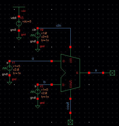
Full-Adder:
Lastly, we combine the NAND and XOR Gates to create a Full-Adder.
Schematic: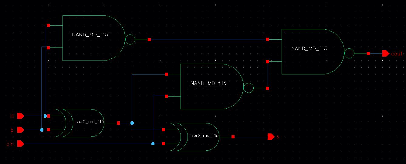
Symbol: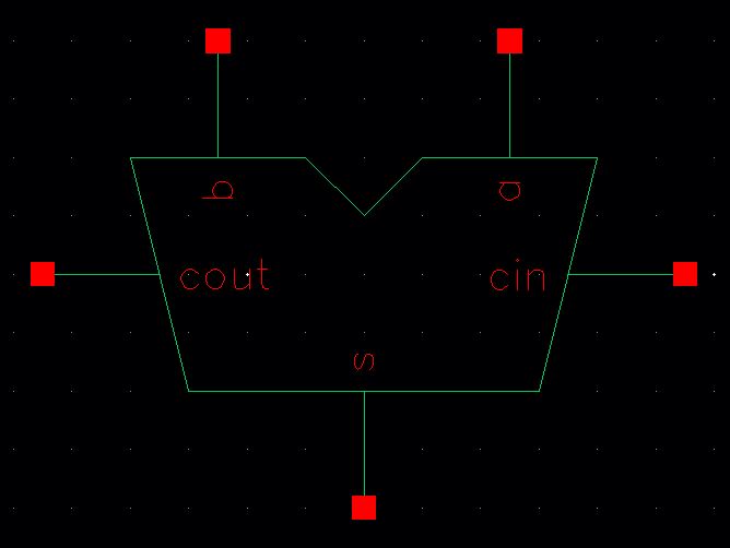
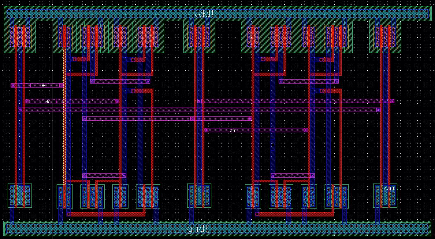
Layout:
The
layout is very tedious and strenuous; thus, be sure to constantly DRC
to verify the design is following appropriate parameters.
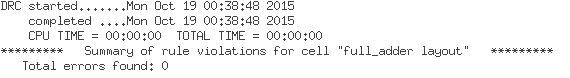
Extracted:
Simulation Schematic:
Unfortunately,
I couldn't get my Full-Adder to simulate; therefore, I won't be able to
show a simulation of my design. That is the only error I had in my lab.
I most likely have issues with my pulse voltages.
Back up files
Afterwards,
it is always important to backup files by either creating a folder on
your personal computer, emailing the files to yourself and/or backing
it up on a cloud (dropbox, icloud, google drive).
Return to my labs
Return to EE421L Labs