Lab 5 - ECE 421L
Degracia, Manuel C.
degracia@unlv.nevada.edu
5 October 2015
Pre-Lab
- Go through Tutorial #3.
- Back-up all work from the lab and the course.
Post-Lab
Objectives:
- Draft schematics, layouts, and symbols for two inverters having sizes of:
- 12u/6u (= width of the PMOS / width of the NMOS with both devices having minimum lengths of 0.6u)
- 48u/24u where the devices use a multiplier, M = 4 (set along with the width and length of the MOSFET).
- Using SPICE simulate the operation of both of your inverters showing each driving a 100 fF, 1 pF, 10 pF, and 100 pF capacitive load
- Comment, in your report, on the results
- Zip up files in Cadence after completion.
Process:
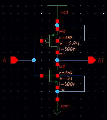
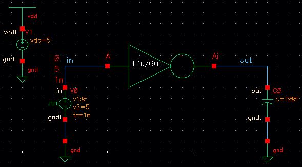
Design a 12u/6u Inverter
1. Design the schematic displayed below. Be sure to Check and Save to ensure there are no issues/errors with the schematic.
2.
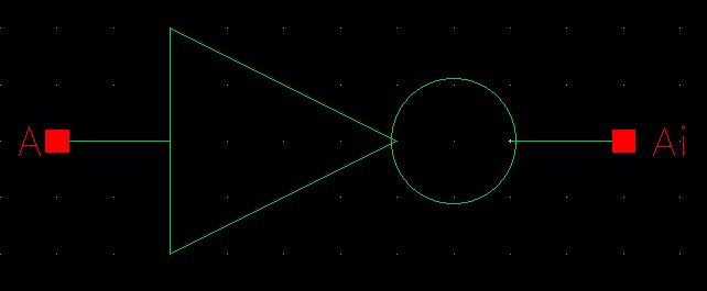
Create the symbol for the 12u/6u inverter (Create > Cell View >
From Cell View). Delete everything but the pins and draw the inverter
(Create > Shape > Line/Circle). Ensure pin positions and
direction. Check and Save.
3.
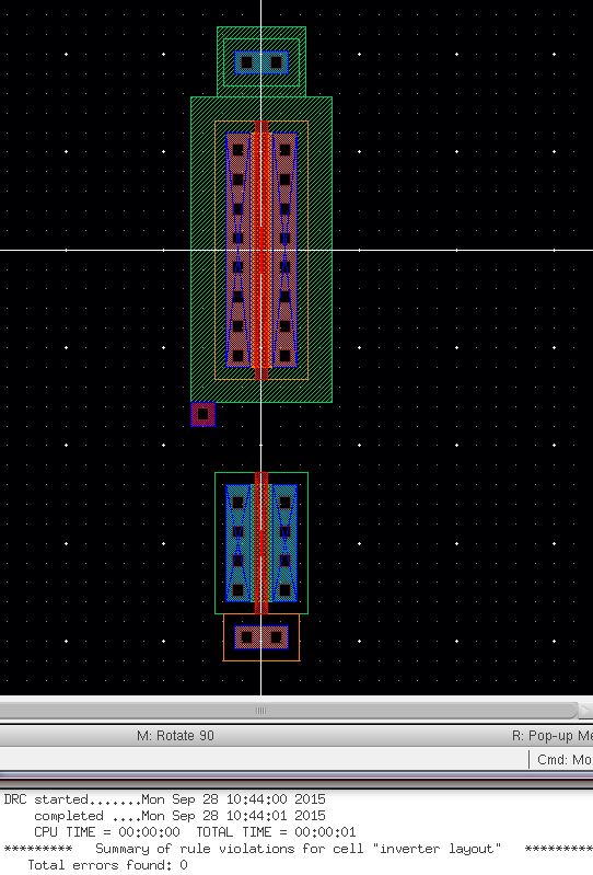
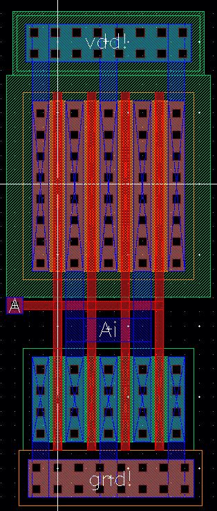
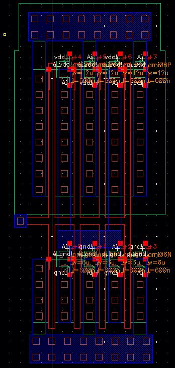
Create the displayed layout view by instantiating the following cells:
nmos, pmos, ntap, ptap and m1_poly. DRC to ensure there are no errors
in placement.
4.
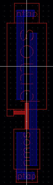
Link the cells using rectangles in the metal1 layer and insert pin
names following the schematic. In the poly layer, connect the nmos to
pmos and m1_poly. DRC/Check and Save.
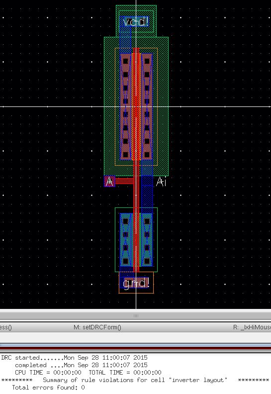
The view below depicts the connections in the metal1 and poly layer.
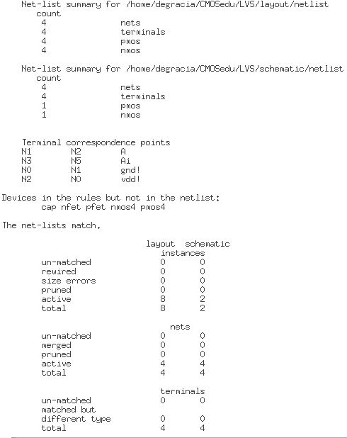
5. DRC and Extract once verified.
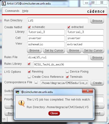
6. LVS to ensure netlists match between the schematic and extracted view.
Design a 48u/24u Inverter w/ a Multiplier of m=4
7.
The inverter for this design is identical to the previous except that
it has a multiplier of m = 4. Due to this, we can just copy the
previous inverter schematic and change the multiplier by 4. In doing
so, it multiplies the width and length by 4 to equate to 48u/24u. 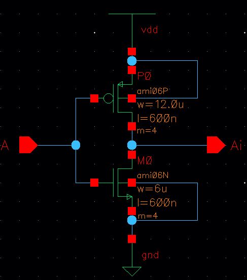
8. Following the same steps as the previous inverter symbol, create the symbol displayed below. 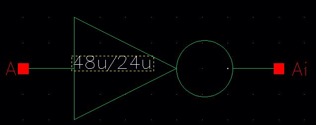
9.
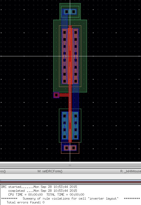
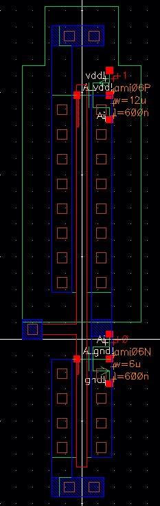
Similar to the previous design, copy the layout and change the
multiplier to 4 resulting in the following layout. Re-adjust
connections in the metal1 and poly layer. DRC/Check and Save.
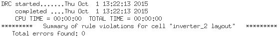
10. Extract the layout once verified and LVS.

Simulations w/ Driving Capacitors (100 fF, 1 pF, 10 pF, 100pF)
Now that the two inverters have been created, we can simulate each one with different capacitors similar to the one below.
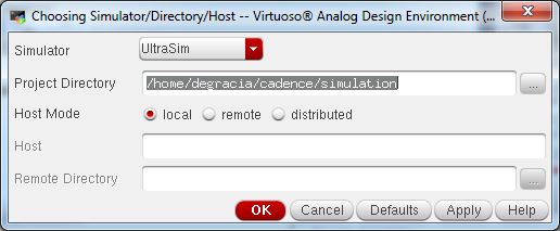
In
these simulations, we will be using UltraSim instead of the usual
Spectre state. UltraSim only performs transient analysis and is used to
perform faster SPICE simulations for larger circuits at the cost of
accuracy.
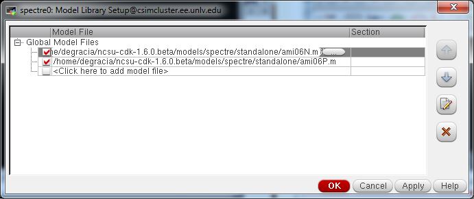
Set model libraries to ami06P.m and ami06N.m.
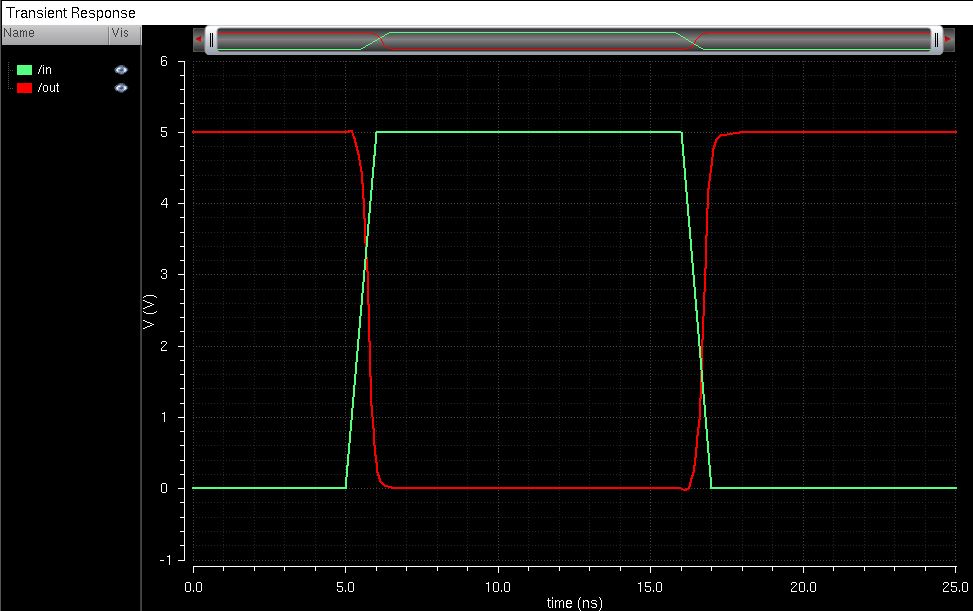
The Transient Responses for each capacitor value is depicted below:
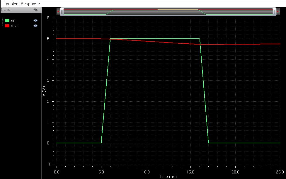
12u/6u C = 100 fF
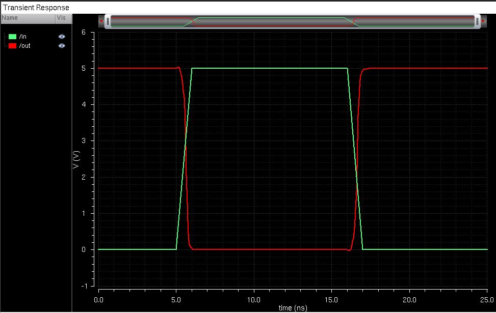
12u/6u C = 1 pF
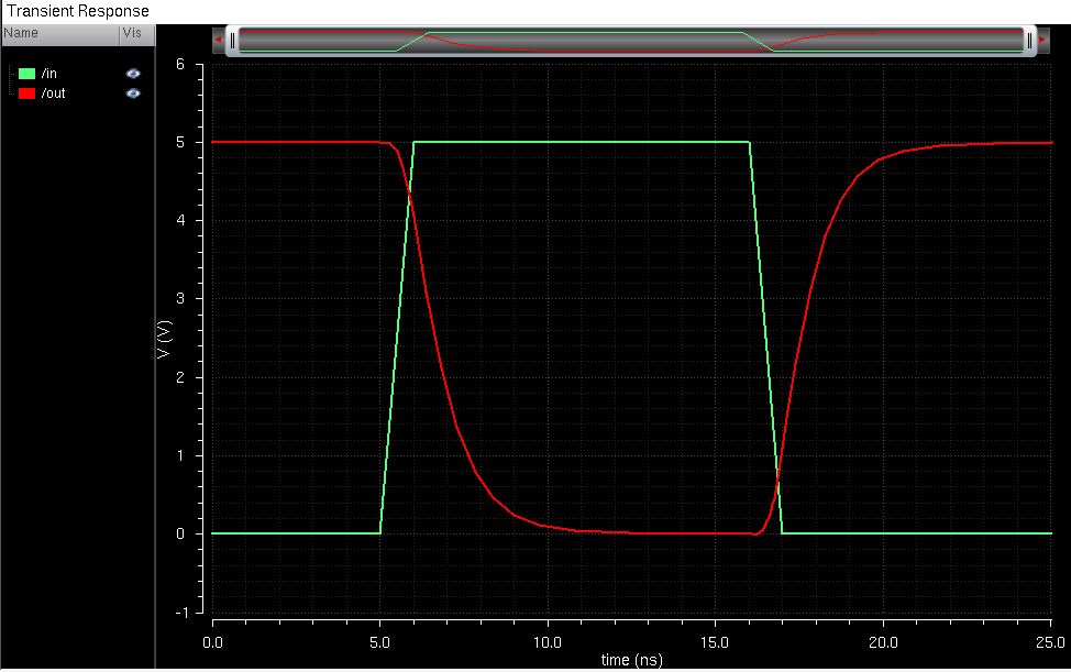
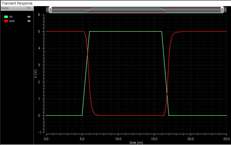
12u/6u C = 10 pF
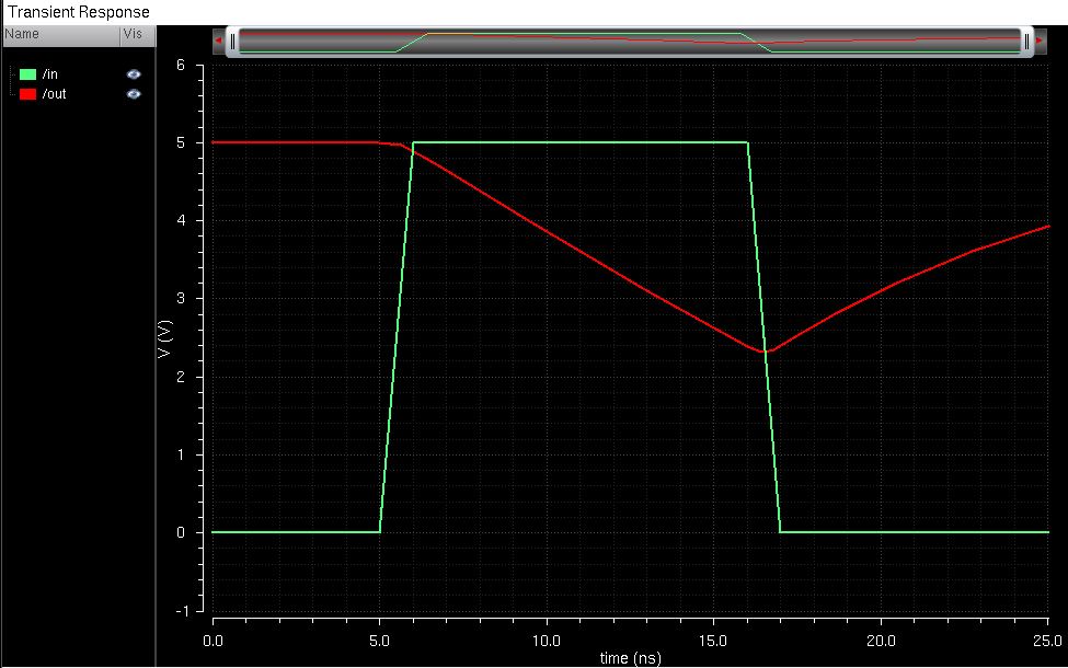
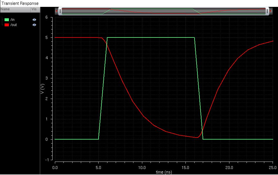
12u/6u C = 100 pF
48u/24u C = 100 fF
48u/24u C = 1 pF
48u/24u C = 10 pF
48u/24u C = 100 pF
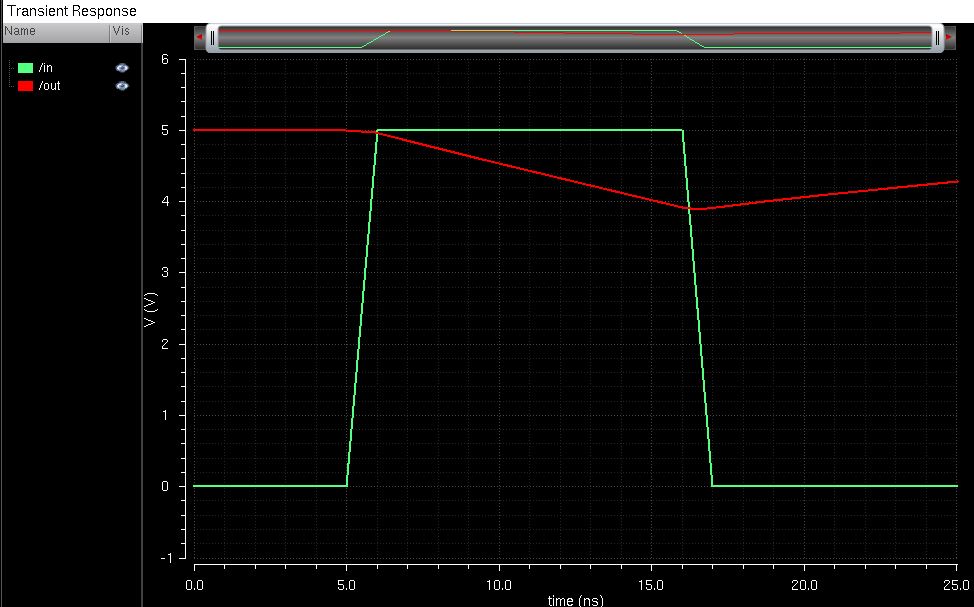
Analyzing
the Transient Responses, one can deduce that as the capacitor value
increases, the fall time for the 12u/6u inverter increases at a faster
rate than the 48u/24u inverter. In addition, as the capacitor value
increases, we can see the output, Ai, become closer to a constant
voltage.
Back up files
Afterwards,
it is always important to backup files by either creating a folder on
your personal computer, emailing the files to yourself and/or backing
it up on a cloud (dropbox, icloud, google drive).

Return to my labs
Return to EE421L Labs