Lab 4 - ECE 421L 

Degracia, Manuel C.

degracia@unlv.nevada.edu

21 September 2015


Pre-Lab


Objectives:


  1. Back-up all of your work from the lab and the course.
  2. Go through Tutorial #2 - Layout and simulating IV curves of PMOS and NMOS devices.
  3. In the simulations in this lab the body of all NMOS devices (the substrate) should be at ground (gnd!) and the body of all PMOS devices  (the n-well) should be at a vdd! of 5V.
 
Tutorial #2 Process:


1. Open MobaXterm and start Cadence in the CMOSedu directory.


2. Create a new library called Tutorial_2 and copy the cellviews from Tutorial_1 using the copy command. Be sure to select the option Update Instances so the cellviews in Tutorial_2 will not reference Tutorial_1. We want Tutorial_2 to be self-contained.


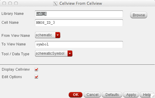
3. Create a schematic cell called NMOS_IV_3. The "3" indicates the use of a 3-terminal transistor.


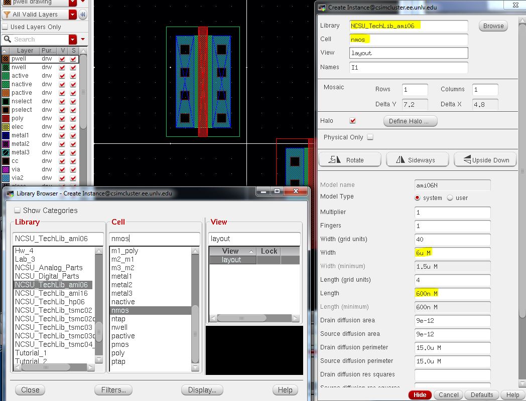
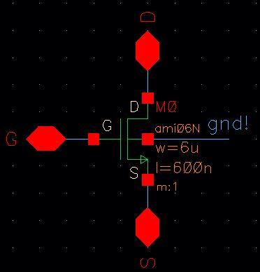
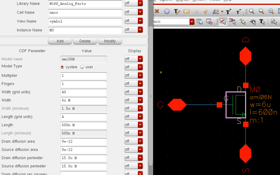
4. Instantiate an nmos from the NCSU_Analog_Parts > N_Transistors library, with a width of Width = 6u and Length = 600n


http://cmosedu.com/jbaker/courses/ee421L/f15/students/degracia/Lab4/Pre-Lab%20Photos/Create%20NMOS%206u%20x%20600n.JPG


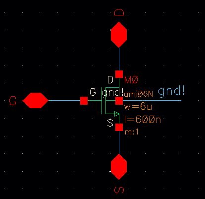
5. Add Pins with the direction set to InputOutput and wires as seen below. Check and Save the schematic when finished. 


http://cmosedu.com/jbaker/courses/ee421L/f15/students/degracia/Lab4/Pre-Lab%20Photos/nmos4.JPG


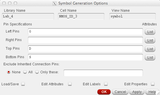
6. From the schematic, create a symbol view (Create > Cellview > From Cellview). Follow through the windows making the necessary changes to ensure the symbol will be created like the one below.


http://cmosedu.com/jbaker/courses/ee421L/f15/students/degracia/Lab4/Pre-Lab%20Photos/NMOS_IV_3%20Symbol.JPG


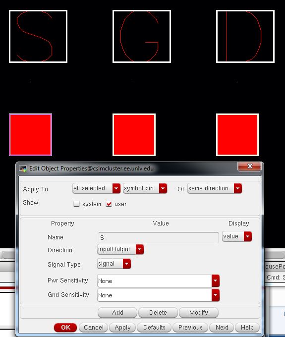
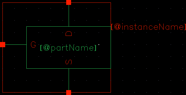
7. Delete everything in the symbol except for the pins. Select all pins and edit their properties with the edit hotkey (q). Select "all selected" and display "value" as seen below.


http://cmosedu.com/jbaker/courses/ee421L/f15/students/degracia/Lab4/Pre-Lab%20Photos/NMOS_IV_3%20Edited%20Symbol.JPG


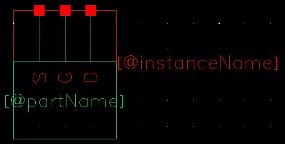
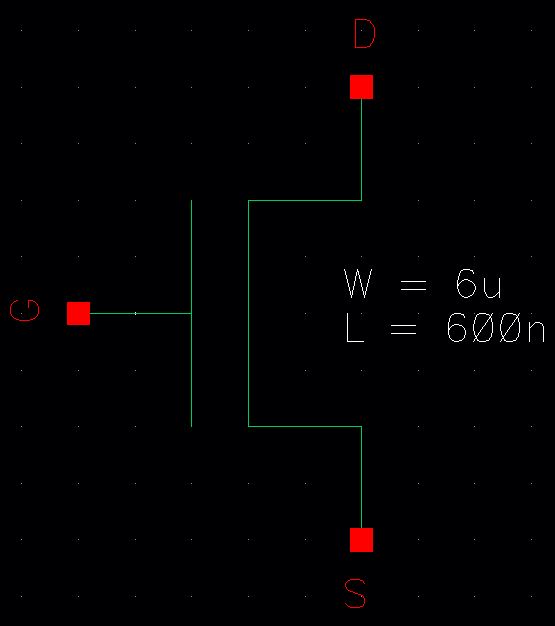
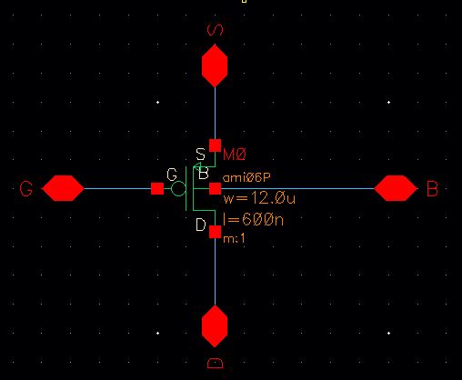
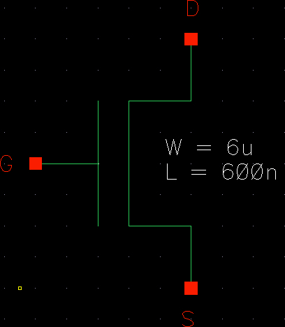
8. Draw a MOSFET symbol and move the pins (rotate if needed) to get a drawing similar to the one displayed. Use commands Create > Shape > Line to draw the lines and Create > Note > Text to include the width and length text.

 
Check and Save


http://cmosedu.com/jbaker/courses/ee421L/f15/students/degracia/Lab4/Pre-Lab%20Photos/Drawn%20NMOS%20Symbol.JPG


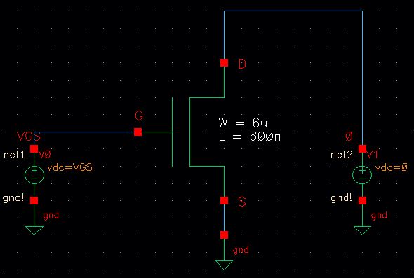
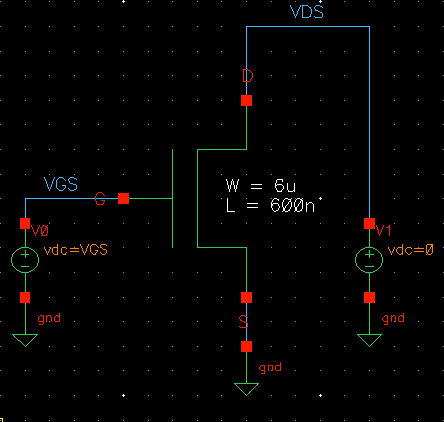
9. Create a schematic cell called sim_NMOS_IV_3. Instantiate the NMOS_IV_3 symbol that was just created and voltage sources. Build the schematic below paying attention to the values of the voltage sources. Check and Save.


http://cmosedu.com/jbaker/courses/ee421L/f15/students/degracia/Lab4/Pre-Lab%20Photos/NMOS_IV_3%20Schematic.JPG


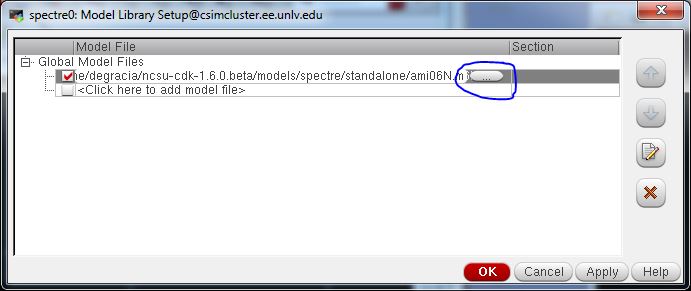
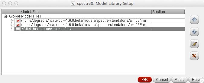
10. Launch ADE and go to Setup > Model Libraries. Set the library to /$HOME /ncsu-cdk-1.6.0.beta/models/spectre/standalone/ami06N.m.


http://cmosedu.com/jbaker/courses/ee421L/f15/students/degracia/Lab4/Pre-Lab%20Photos/Model%20Library%20Setup.JPG


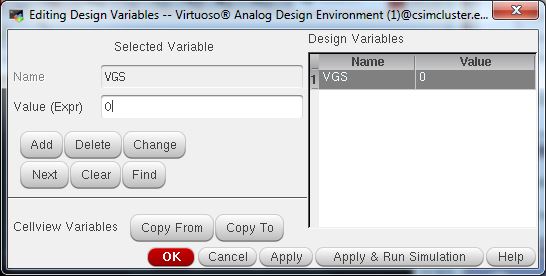
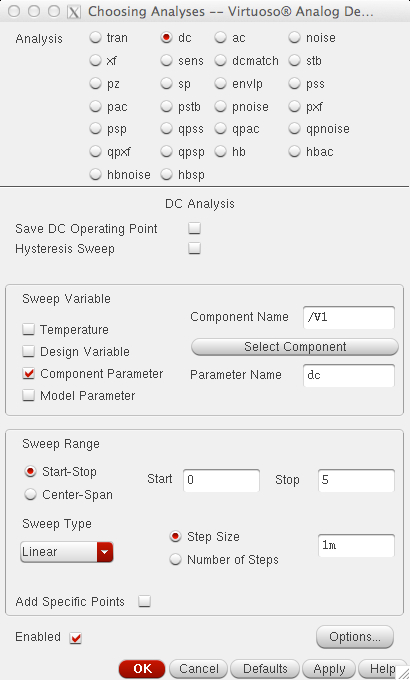
11. In the ADE window, select Variables > Edit, and add VGS = 0 as a parameter.


http://cmosedu.com/jbaker/courses/ee421L/f15/students/degracia/Lab4/Pre-Lab%20Photos/Edit%20Design%20Variables.JPG


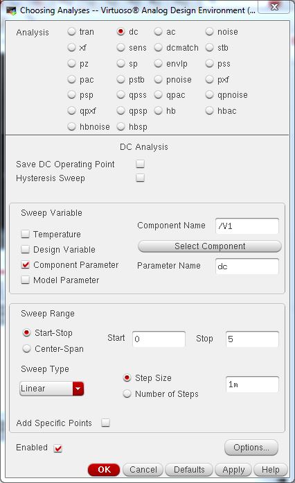
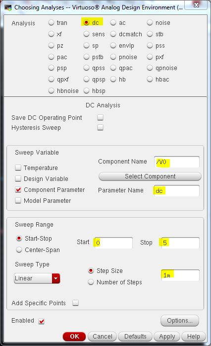
12. Set the Analysis as displayed below.


http://cmosedu.com/jbaker/courses/ee421L/f15/students/degracia/Lab4/Pre-Lab%20Photos/Choosing%20Analysis.JPG


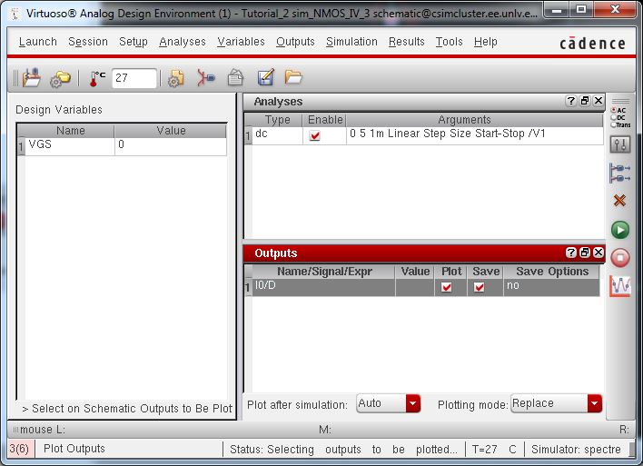
13. Select Output > To Be Plotted > Select on Schematic. Choose the D pin to be plotted for its current analysis. 


http://cmosedu.com/jbaker/courses/ee421L/f15/students/degracia/Lab4/Pre-Lab%20Photos/Simulation%20Parameters.JPG


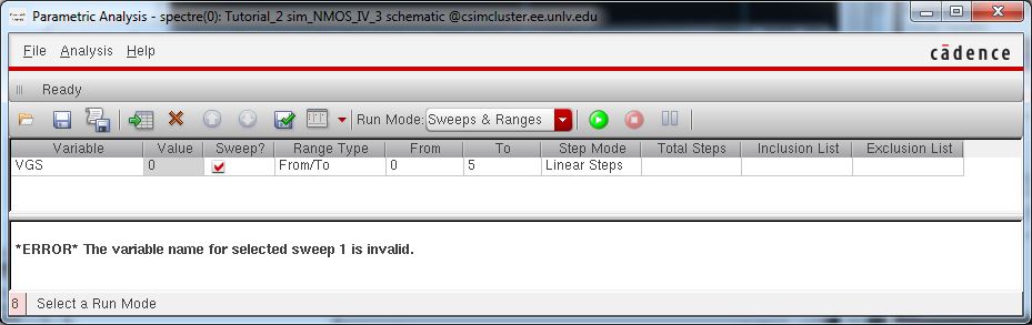
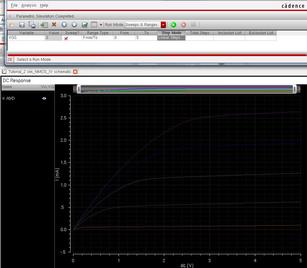
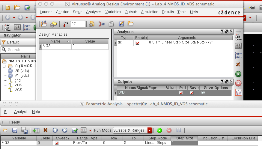
15. Lastly, choose Tools > Parametric Analysis and set the parameters seen below. Click the Green button with an arrow inside to start the Parametric Analysis and simulate the MOSFET IV curves.


http://cmosedu.com/jbaker/courses/ee421L/f15/students/degracia/Lab4/Pre-Lab%20Photos/Parametric%20Analysis.JPG


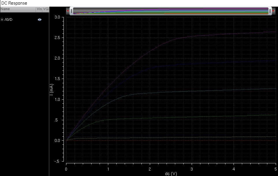
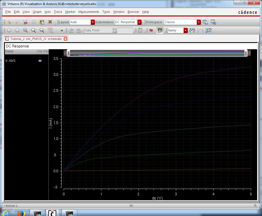
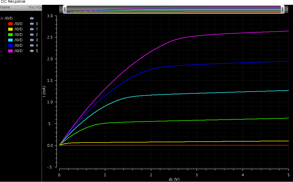
16. Save the simulation state in the cellview. The DC Response should look like the one below.


http://cmosedu.com/jbaker/courses/ee421L/f15/students/degracia/Lab4/Pre-Lab%20Photos/DC%20Response.JPG


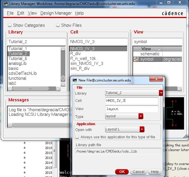
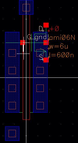
17. Close all cellviews. Create a layout view for NMOS_IV_3.


http://cmosedu.com/jbaker/courses/ee421L/f15/students/degracia/Lab4/Pre-Lab%20Photos/NMOS_IV_3%20Layout.JPG


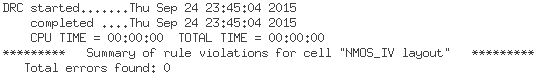
18. Instantiate an nmos device that is 6um wide and 600nm long, ptap cell (metal1 connection to p+). DRC the layout.


http://cmosedu.com/jbaker/courses/ee421L/f15/students/degracia/Lab4/Pre-Lab%20Photos/Insert%20ptap.JPG


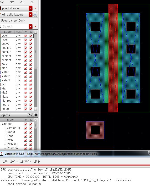
19. Instatiate a metal1-connection-to-poly cell (m1_poly). In the metal1 layer, add rectangles to connect the source to the p-substrate and the the drain. In the poly layer, add a rectangle to connect the gate to m1_poly. DRC the layout.


http://cmosedu.com/jbaker/courses/ee421L/f15/students/degracia/Lab4/Pre-Lab%20Photos/Insert%20m1_poly.JPG


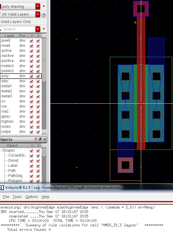
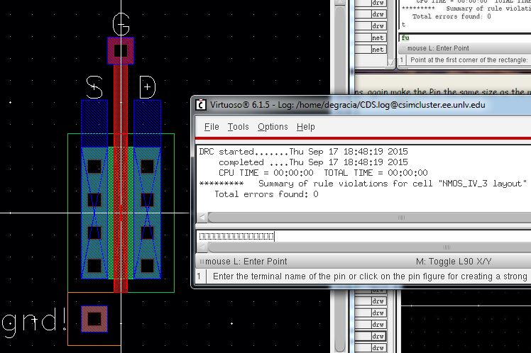
20. Add D, G, and S pins on the metal1 layer with I/O type set to InputOutput as seen below. DRC once again and Save the cell.


http://cmosedu.com/jbaker/courses/ee421L/f15/students/degracia/Lab4/Pre-Lab%20Photos/NMOS%20Updated%20Pin%20Names.JPG


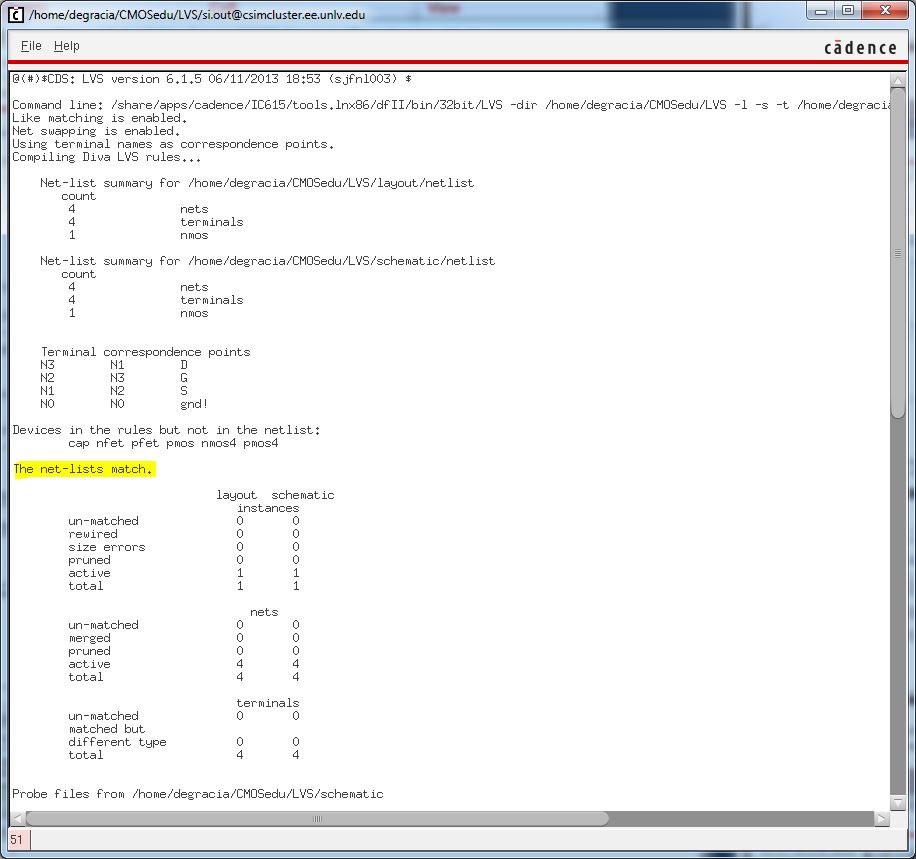
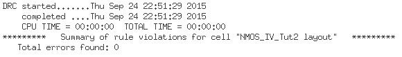
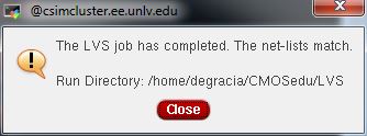
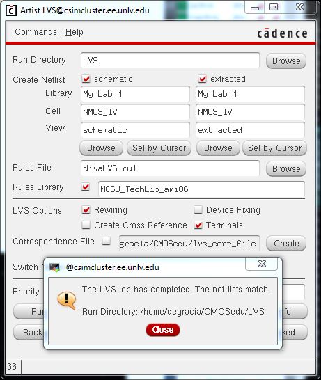
21. Once DRC finds no errors, extract the layout and open the extracted view. Then LVS the extracted view.


http://cmosedu.com/jbaker/courses/ee421L/f15/students/degracia/Lab4/Pre-Lab%20Photos/LVS.JPG


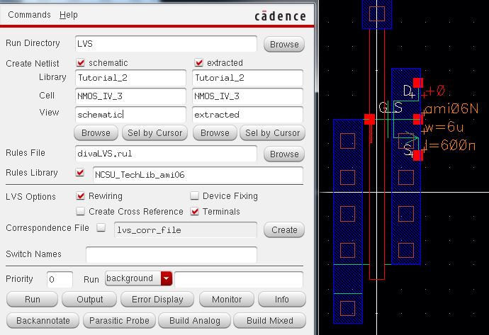
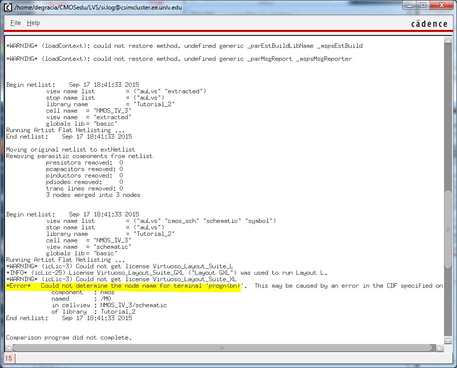
22. An error will be displayed. The error is related to the bulk (p-substrate) connection for the NMOS. Again, as mentioned above when the 3 terminal MOSFET symbol is used it’s assumed that the bulk is tied to gnd! for an NMOS device and vdd! for a PMOS device.


http://cmosedu.com/jbaker/courses/ee421L/f15/students/degracia/Lab4/Pre-Lab%20Photos/LVS%20Error%20Netlist.JPG


23. Delete the metal1 rectangle and S pin to the ptap. Add seperate rectangles on S and B metal. Save and DRC.


http://cmosedu.com/jbaker/courses/ee421L/f15/students/degracia/Lab4/Pre-Lab%20Photos/NMOS%20Updated%20Pin%20Names.JPG


24. Run the extractor and open the extracted view. LVS it again and errors will still be displayed.


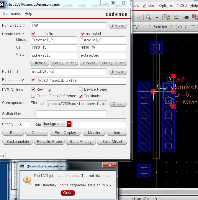
25. Open the Library Manager and rename NMOS_IV_3 to NMOS_IV. Also, rename sim_NMOS_IV_3 to sim_NMOS_IV. Now open the schematic view of NMOS_IV and change the NMOS symbol to nmos4 for 4 pins.


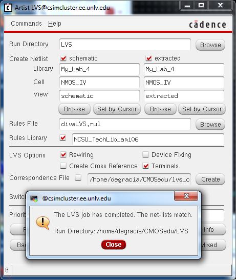
26. Open the extracted view and perform an LVS. The LVS should have no errors this time around do the the change from nmos to nmos4.


http://cmosedu.com/jbaker/courses/ee421L/f15/students/degracia/Lab4/Pre-Lab%20Photos/LVS%20NMOS_IV.JPG


http://cmosedu.com/jbaker/courses/ee421L/f15/students/degracia/Lab4/Pre-Lab%20Photos/LVS%20NMOS_IV%20Output.JPG


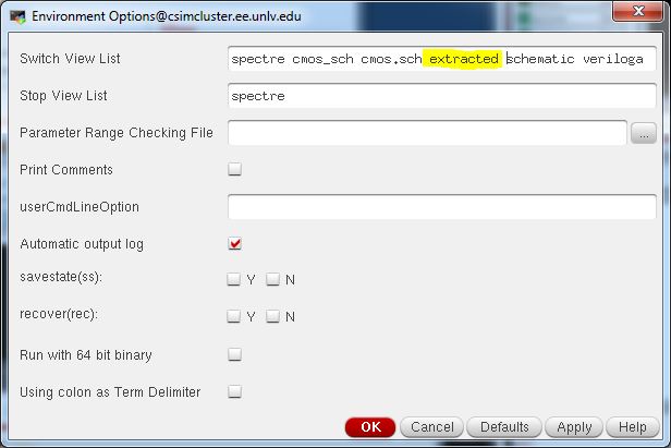
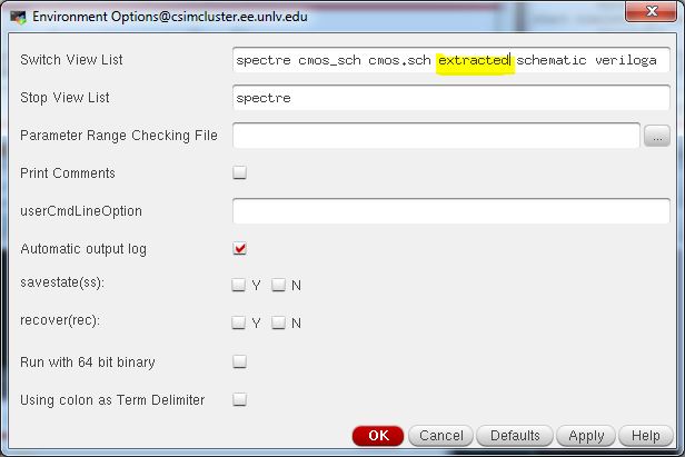
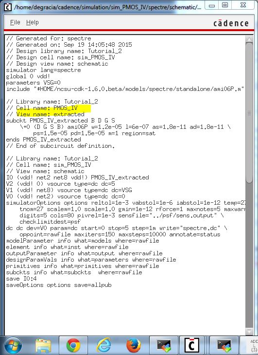
27. Simulate the extracted layout. Open the schematic view of sim_NMOS_IV and then launch ADE L. Run through the same process as earlier with only one change. Select  Setup > Environment and enter "extracted" before "schematic" so the extracted view is used before the schematic view when initiated.


http://cmosedu.com/jbaker/courses/ee421L/f15/students/degracia/Lab4/Pre-Lab%20Photos/ADE%20Environment%20Setup.JPG


28. Run the Parametric Analysis, which should display the same DC Response graph.


http://cmosedu.com/jbaker/courses/ee421L/f15/students/degracia/Lab4/Pre-Lab%20Photos/Same%20DC%20Response.JPG


PMOS Device (Similiar to the NMOS Device)


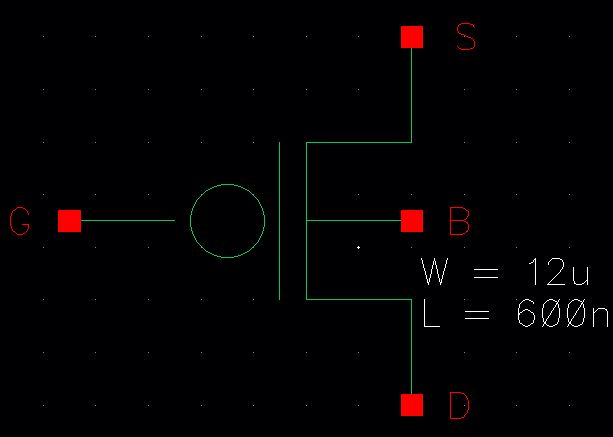
29. Create a schematic Cell View called PMOS_IV with 4 pins as seen below. Note the W and L of the PMOS device. Check and Save.


http://cmosedu.com/jbaker/courses/ee421L/f15/students/degracia/Lab4/Pre-Lab%20Photos/PMOS.JPG


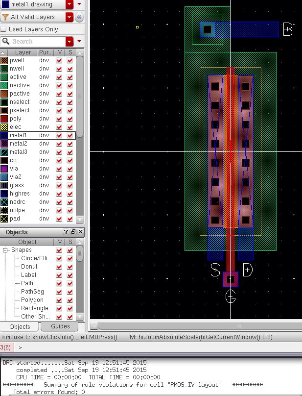
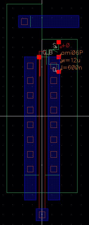
30. Create a symbol for the schematic. Check and Save.


http://cmosedu.com/jbaker/courses/ee421L/f15/students/degracia/Lab4/Pre-Lab%20Photos/PMOS%20Symbol.JPG


31. Create a layout and instantiate a pmos cell, m1_poly and ntap. Draw the metal1 rectangles and Pins as displayed below. DRC and Save the layout.


http://cmosedu.com/jbaker/courses/ee421L/f15/students/degracia/Lab4/Pre-Lab%20Photos/PMOS_IV%20Layout%20DRC.JPG


32. Extract the layout and open the extracted view. Save and close all cellviews.


http://cmosedu.com/jbaker/courses/ee421L/f15/students/degracia/Lab4/Pre-Lab%20Photos/PMOS_IV%20Extracted.JPG 


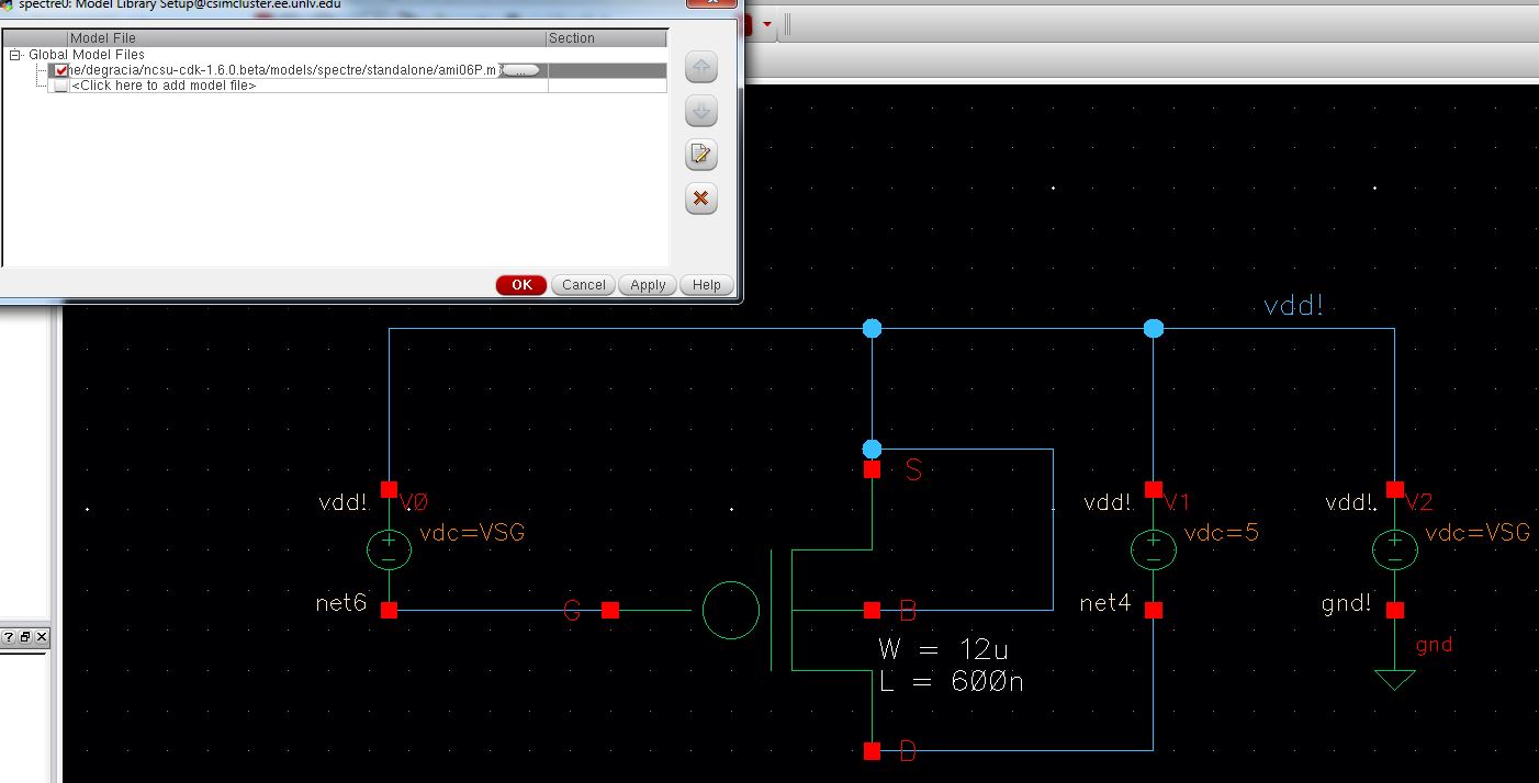
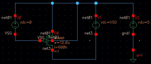
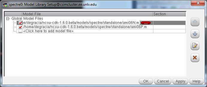
33. Next create a cell called sim_PMOS_IV and draft the following schematic. Note the value of /V1 is VSG (not VGS as we used in the NMOS sim). Check and Save. 


http://cmosedu.com/jbaker/courses/ee421L/f15/students/degracia/Lab4/Pre-Lab%20Photos/sim_PMOS_IV%20schematic.JPG


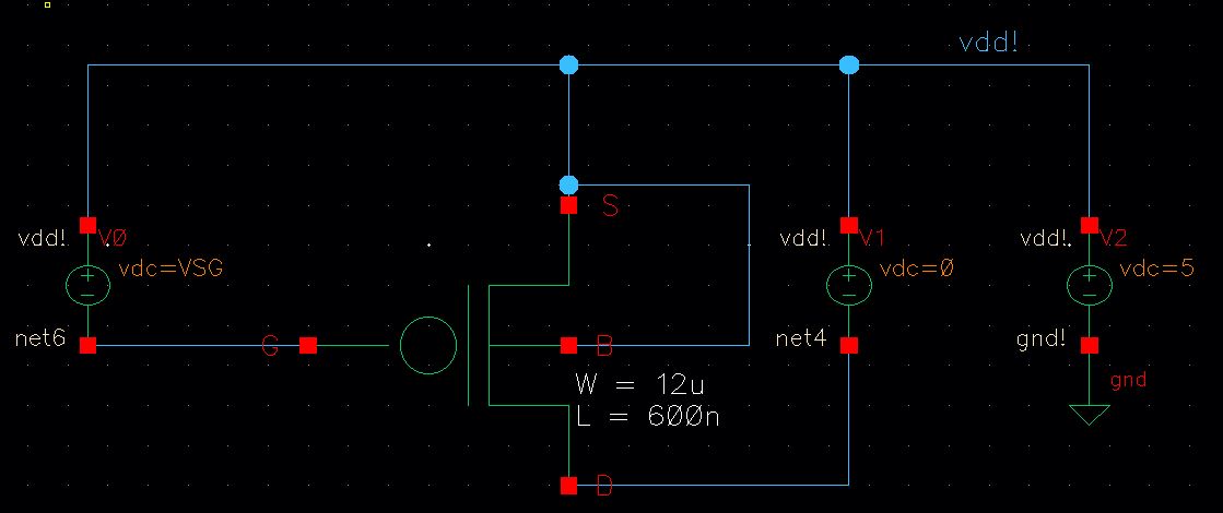
34. Launch the ADE then go to Setup > Model Libraries and select the PMOS models for AMI06P.m. Then go to Variables -> Edit and Add VSG with a value of 0 (not VGS).


http://cmosedu.com/jbaker/courses/ee421L/f15/students/degracia/Lab4/Pre-Lab%20Photos/PMOS%20Model%20Library%20Setup.JPG


35. Go through the same process for simulation as we did for the NMOS in the previous steps. This includes adding "extracted" before "schematic"in the enviroment options. 


http://cmosedu.com/jbaker/courses/ee421L/f15/students/degracia/Lab4/Pre-Lab%20Photos/PMOS%20Analysis%20Setup.JPG

http://cmosedu.com/jbaker/courses/ee421L/f15/students/degracia/Lab4/Pre-Lab%20Photos/PMOS_IV%20Extracted%20DC%20Analysis.JPG

http://cmosedu.com/jbaker/courses/ee421L/f15/students/degracia/Lab4/Pre-Lab%20Photos/PMOS_IV%20DC%20Analysis.JPG

http://cmosedu.com/jbaker/courses/ee421L/f15/students/degracia/Lab4/Pre-Lab%20Photos/PMOS%20Extracted%20Netlist.JPG

Back up files
 
Afterwards, it is always important to backup files by either creating a folder on your personal computer, emailing the files to yourself and/or backing it up on a cloud (dropbox, icloud, google drive).


http://cmosedu.com/jbaker/courses/ee421L/f15/students/degracia/Lab4/Pre-Lab%20Photos/Back%20up.JPG


Post-Lab


Overview:

Process:
 
ID v. VDS of an NMOS Device
 
1. As discussed and worked out in the Pre-lab and/or Tutorial #2, create the NMOS shown below with the given parameters.
 http://cmosedu.com/jbaker/courses/ee421L/f15/students/degracia/Lab4/Post-Lab%20Photos/1.-Add-Nmos-Instance.jpg


2. Create a symbol from the schematic (Create > Cellview > From Cellview) and set the pins based on the topology of the schematic above.


http://cmosedu.com/jbaker/courses/ee421L/f15/students/degracia/Lab4/Post-Lab%20Photos/2.-Create-NMOS-Symbol.jpg

http://cmosedu.com/jbaker/courses/ee421L/f15/students/degracia/Lab4/Post-Lab%20Photos/3.-Set-Pins.jpg


3. From the new symbol


http://cmosedu.com/jbaker/courses/ee421L/f15/students/degracia/Lab4/Post-Lab%20Photos/4.-Symbol-Creation.jpg

 http://cmosedu.com/jbaker/courses/ee421L/f15/students/degracia/Lab4/Post-Lab%20Photos/5.-Editted-Symbol.jpg


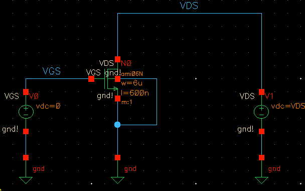
4. With the new symbol created, open a new schematic and create the one below following the guidelines in the overview.


http://cmosedu.com/jbaker/courses/ee421L/f15/students/degracia/Lab4/Post-Lab%20Photos/6.-NMOS-ID_VDS-Schematic.jpg 


5. Launch ADE L for simulation and setup the model libraries to the ones displayed (Setup > Model Libraries). In most cases, the only library needed would be for the device you are simulating, NMOS or PMOS, but I put both in as a habit for when we will start create schematics with both.


http://cmosedu.com/jbaker/courses/ee421L/f15/students/degracia/Lab4/Post-Lab%20Photos/7.-Model-Libraries.jpg


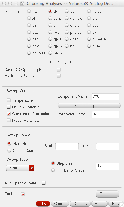
6. Setup the DC Analysis in which we set the values of VDS using "Component Parameters."


http://cmosedu.com/jbaker/courses/ee421L/f15/students/degracia/Lab4/Post-Lab%20Photos/8.-DC-Analysis-Parameters.jpg


7. Since we want to plot different values of VGS as well, we will have to do a Parametric Analysis (Tools > Parametric Analysis).

Click the "Green Button" in Parametric Analysis to being the simulation.
 

http://cmosedu.com/jbaker/courses/ee421L/f15/students/degracia/Lab4/Post-Lab%20Photos/9.-Parametric-Analysis.jpg


http://cmosedu.com/jbaker/courses/ee421L/f15/students/degracia/Lab4/Post-Lab%20Photos/10.-ID_VDS-DC-Response.jpg


ID v. VGS of an NMOS Device

 
8. Create the following schematic in a new cellview. The difference between this schematic and the previous is the use of the nmos4 symbol.
 

http://cmosedu.com/jbaker/courses/ee421L/f15/students/degracia/Lab4/Post-Lab%20Photos/11.-NMOS-ID_VGS-Schematic.jpg


9.  Launch ADE L and setup the DC Analysis.
 

http://cmosedu.com/jbaker/courses/ee421L/f15/students/degracia/Lab4/Post-Lab%20Photos/12.-DC-Analysis-Parameters.jpg

http://cmosedu.com/jbaker/courses/ee421L/f15/students/degracia/Lab4/Post-Lab%20Photos/13.-ADE-L.jpg


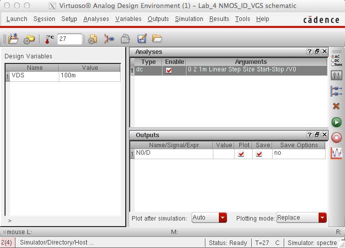
10.  Setup the Model Libraries like earlier.
 
*Because VDS is a set value, we do not have not run the Parametric Analysis like earlier.
 

http://cmosedu.com/jbaker/courses/ee421L/f15/students/degracia/Lab4/Post-Lab%20Photos/14.-Model-Libraries.jpg

http://cmosedu.com/jbaker/courses/ee421L/f15/students/degracia/Lab4/Post-Lab%20Photos/15.-ID_VGS-DC-Response.jpg


ID v. VSD of a PMOS Device

 
11. Create a new schematic cellview and build the schematic below using the PMOS device created in the Pre-Lab and/or Tutorial #2.
 

http://cmosedu.com/jbaker/courses/ee421L/f15/students/degracia/Lab4/Post-Lab%20Photos/16.-PMOS-ID_VSD-Schematic.jpg


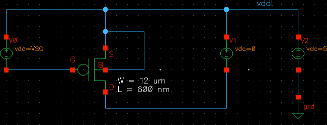
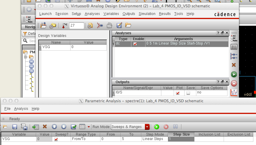
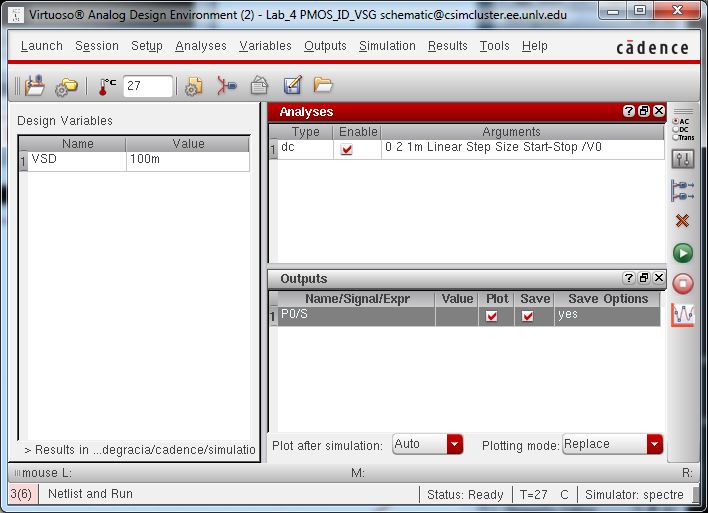
12. Launch ADE L and setup according to the pictures below. Be sure to also set the Model Libraries. 

http://cmosedu.com/jbaker/courses/ee421L/f15/students/degracia/Lab4/Post-Lab%20Photos/17.-Parametric-Analysis.jpg


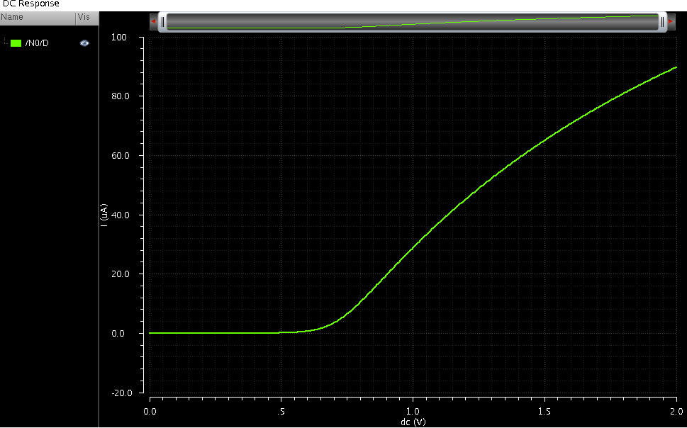
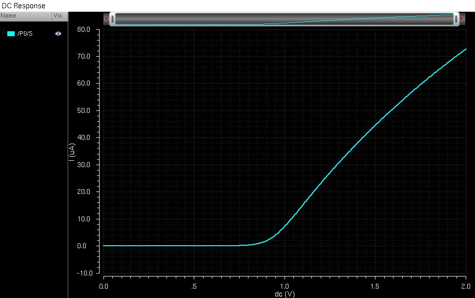
The following DC Response should be displayed, similar to the ID v. VDS of an NMOS device in the first analysis.
 

http://cmosedu.com/jbaker/courses/ee421L/f15/students/degracia/Lab4/Post-Lab%20Photos/18.-PMOS-ID_VSD-DC-Response.jpg


ID v. VSG of a PMOS device

 
13. Create a new schematic cellview and create the following schematic. Be sure to use the pmos4 symbol instead of the pmos symbol we created.
 

http://cmosedu.com/jbaker/courses/ee421L/f15/students/degracia/Lab4/Post-Lab%20Photos/19.%20PMOS%20ID_VSG%20Schematic.JPG


14. Setup the Model Libraries once again and the following parameters for the DC Analysis.


http://cmosedu.com/jbaker/courses/ee421L/f15/students/degracia/Lab4/Post-Lab%20Photos/20.%20Model%20Libraries.JPG

http://cmosedu.com/jbaker/courses/ee421L/f15/students/degracia/Lab4/Post-Lab%20Photos/21.%20PMOS%20ID_VSG%20DC%20Analysis.JPG


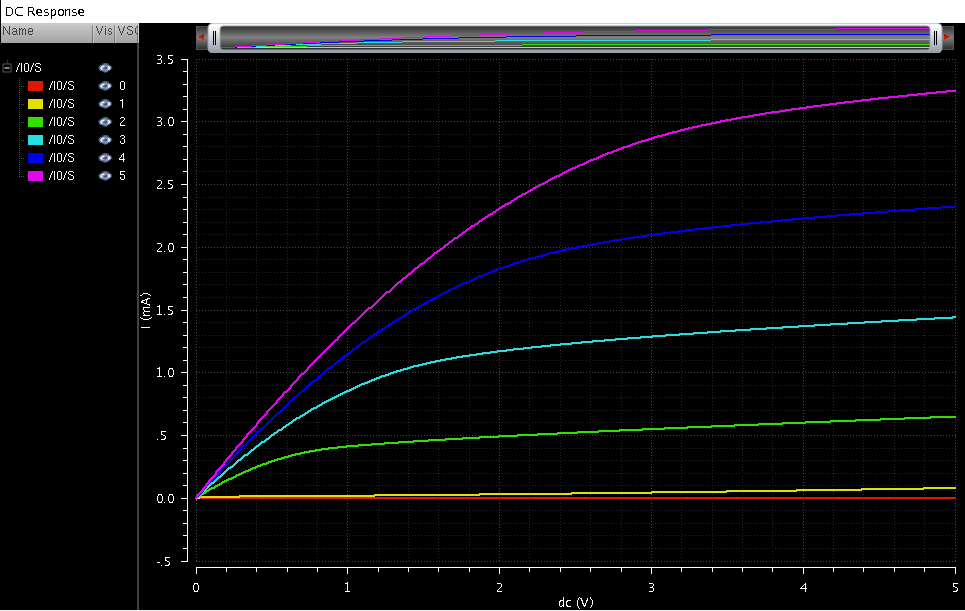
15. The following response will then be shown.

http://cmosedu.com/jbaker/courses/ee421L/f15/students/degracia/Lab4/Post-Lab%20Photos/22.%20PMOS%20ID_VSG%20DC%20Response.JPG


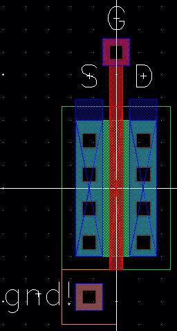
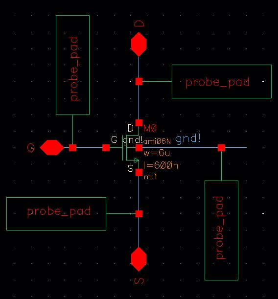
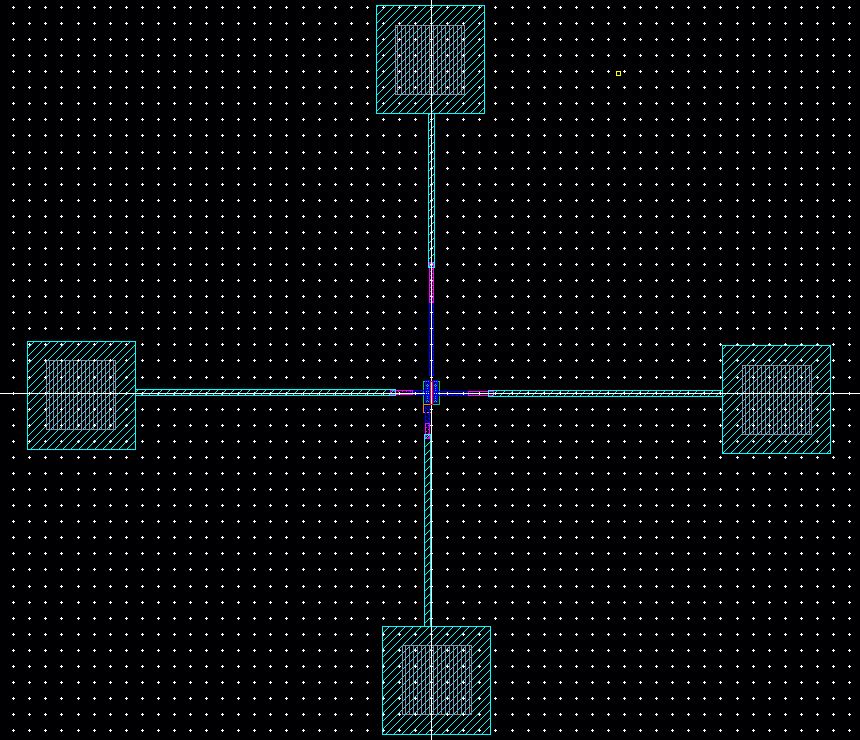
Layout a 6u/0.6u NMOS Device w/ 4 Probe Pads

 
16. Using the NMOS Device we built in the Pre-Lab and/or Tutorial #2, DRC, Extract and LVS once more to double check for errors.
   
Layout

http://cmosedu.com/jbaker/courses/ee421L/f15/students/degracia/Lab4/Post-Lab%20Photos/23.%20NMOS%20Layout.JPG


DRC

http://cmosedu.com/jbaker/courses/ee421L/f15/students/degracia/Lab4/Post-Lab%20Photos/24.%20NMOS%20Layout%20DRC.JPG


Schematic

http://cmosedu.com/jbaker/courses/ee421L/f15/students/degracia/Lab4/Post-Lab%20Photos/25.%20NMOS%20Schematic.JPG 


Extracted

http://cmosedu.com/jbaker/courses/ee421L/f15/students/degracia/Lab4/Post-Lab%20Photos/26.%20NMOS%20Extracted.JPG


LVS

http://cmosedu.com/jbaker/courses/ee421L/f15/students/degracia/Lab4/Post-Lab%20Photos/27.%20NMOS%20LVS.JPG


17. Open up the schematic once more and instantiate probe pads to each corresponding pins.
 

http://cmosedu.com/jbaker/courses/ee421L/f15/students/degracia/Lab4/Post-Lab%20Photos/28.%20NMOS%20w%20Probe%20pad.JPG


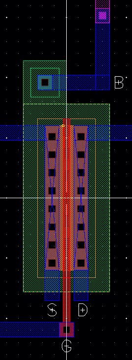
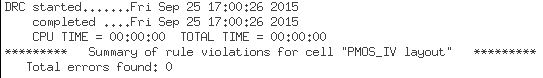
18. Open the layout of the NMOS and following the topology of the schematic, instantiate 4 probe pads and connect them using the appropriate connecters and layers. DRC to make sure you do not encounter any errors such as spacing or layer issues.
 

http://cmosedu.com/jbaker/courses/ee421L/f15/students/degracia/Lab4/Post-Lab%20Photos/29.%20NMOS%20w%20Probe%20pab%20layout.JPG


http://cmosedu.com/jbaker/courses/ee421L/f15/students/degracia/Lab4/Post-Lab%20Photos/30.%20DRC.JPG


19. Extract the layout and LVS to ensure netlists match.


http://cmosedu.com/jbaker/courses/ee421L/f15/students/degracia/Lab4/Post-Lab%20Photos/31.%20LVS.JPG


Layout a 12u/0.6u PMOS Device w/ 4 Probe Pads

 
20.  Similiar to the NMOS Device, we will use the PMOS Device built in the Pre-lab and/or Tutorial #2. Instantiate probe pads to each of the following pins.
   

http://cmosedu.com/jbaker/courses/ee421L/f15/students/degracia/Lab4/Post-Lab%20Photos/35.%20PMOS%20Schematic.JPG


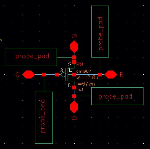
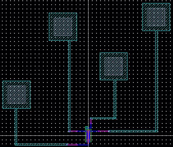
21. Open up the layout of the PMOS Device and instantiate probe pads following the topology above.


http://cmosedu.com/jbaker/courses/ee421L/f15/students/degracia/Lab4/Post-Lab%20Photos/33.%20PMOS%20w%20Probe%20pad%20Zoomed.JPG 


Connect them using the appropriate connecters and layers. DRC to make sure you do not encounter any errors such as spacing or layer issues.


http://cmosedu.com/jbaker/courses/ee421L/f15/students/degracia/Lab4/Post-Lab%20Photos/32.%20PMOS%20w%20Probe%20pad.JPG


http://cmosedu.com/jbaker/courses/ee421L/f15/students/degracia/Lab4/Post-Lab%20Photos/34.%20DRC.JPG


22. Extract the layout and LVS to ensure netlists match.
   

http://cmosedu.com/jbaker/courses/ee421L/f15/students/degracia/Lab4/Post-Lab%20Photos/36.%20LVS.JPG


Back up files
   
Afterwards, it is always important to backup files by either creating a folder on your personal computer, emailing the files to yourself and/or backing it up on a cloud (dropbox, icloud, google drive).


http://cmosedu.com/jbaker/courses/ee421L/f15/students/degracia/Lab4/Post-Lab%20Photos/37.%20Back%20up.JPG


Return to my labs


Return to EE421L Labs