EE 421L - Lab 2-Design of a 10-Bit Digital-to-Analog Converter (DAC)

Jonathan K DeBoy
deboyj@unlv.nevada.edu
31 August 2015


Pre-lab work


Introduction

This lab to use the Cadence EDA tools to implement our 10-bit digital-to-analog converter (DAC) design using n-well resistors. This is schematic and simulations only, layout is left for the following week.


Prelab Work

Below is the schematic that is used to test both the ideal DAC and ADC. An analog signals is generated from a source at 2MHz and is fed into the input of the ADC. The ADC performs a conversion with a series of comparaters or switches and outputs a 10-bit digital value. That 10-bit bus is fed into the DAC which makes use of switches to generate an analog voltage proportional to the digital value it is recieving. The smallest step size of this limited resolution ideal DAC is given by VDD/2^n where n is the number of bits. By this formula, we can have a resolution of 4.8mV per bit for a 5V supply. This value is also known as our least significant bit (LSB) which is the minimum input voltage change it takes for ouroutput to change.
 
 IdealSim
Simulation Schematic of Ideal ADC and DAC with 2MHz Sinwave Input.
 
Below is an inside look of the ideal DAC  with all of its switches (seen in every DAC_Bit block).
IdealBit     idealDAC
                  Single Bit of Ideal DAC (Switches)                                                                                 Ideal DAC Schematic
 
 Plotting the simulation will result in the following waveform where the input is a clear, analog, continuous-time sinewave and the output is a digital (discrete in voltage levels), continuous-time signal that follows the input curve. The update speed (width of steps) is due to the speed of the clock.
 
idealsim
Simulation of the Above, Ideal Design


10-Bit DAC Design and Simulation


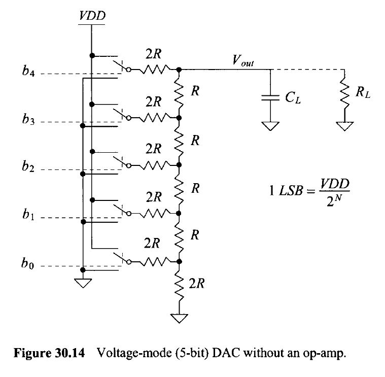
Below is the schematic and output resistance derivation of a simple resistor DAC. Each DAC bit/cell is similar so they all reduce down to 2R.
SimpleDAC     outputresistance
 
 
 Below is a single resistor block that will be repeated to implement our DAC. We only need the footprint of a single 10k n-well resistor since our 2R values are made with two R resistors in series. Next to the schematic is the symbol.
resblock      resblocksym
 
 
This is the schematic of our 10-bit DAC which uses 10 of the above resistor blocks:
MyDAC
 
 
In order to make a symbol file with the same footprint as the ideal DAC provided, we simply copy the cell over and alter the symbol file by removing the VDD, Vref, and ground pins, leaving only our 10 digital inputs and our Vout.
MyDACsym
 
 
MyDACsimschem
Simulation of our 10-Bit DAC. Same as Prelab Simulation (now with our DAC)
 
 
NoLoadSim
This is the simulation waveform for our DAC. Notice how the descrite steps follow the input voltage waveform.
   
 
To find the delay of our DAC, lets apply a pulse to B9 (our voltage should go to 2.5V), and let us find out how long it takes for our output to slew to 50% of that value (1.25V) driving a 10pF loading capacitor. We can estimate that the delay will be 0.7 * 10k * 10p = 70ns. Below is a simulation:
delay_simschem     dealy
 

  Our DAC Driving Different Loads

10k LoadDriving a load of 10k (same as our output resistance) will result in an ouput waveform of have the voltage present at the input.
10pF LoadDriving a capacitive load of 10pF will result in having our steps smooth out, looking more like a proper analog waveform. This will also induce slewing as we can see from the 75ns delay (75n/500n*360= 54 degrees phase shift)
10k&10pF LoadThis time, we are driving both a 10k resistor and a 10pF capacitor, leaving us with a delay of 50ns => 36 degrees phase shift. We also have a lot less voltage since we are diving an additional resistor from the last simulation.
 
 If the DAC was implemented with transistors with a very large switching resistance, then we would have a high impedance input, meaning that the voltage that we are sampling will not go under loading effects since the DAC will draw minimal amounts of current.

Return
Return to EE421L Student Directory
Return to EE421L Page
Return to CMOSedu