Project - ECE 421L
See the EE421L webpage here
Authored by Juan Buendia
buendiaj@unlv.nevada.edu
November 8, 2015
Objective: To learn how to implement various logic gates to create an eight-bit resettable (input"clear") up/down counter
One
of the ways to implement a resettable (input "clear") up/down counter
is by using edge-triggerted D flip-flops with a clear, and it will also
make the countter edge triggered. Implementing edge triggered
clocks allows the user to change its input without affecting the output
untill there is either a rising edge or a falling edge of the clock.
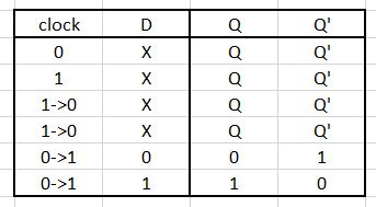
A D flip-flop is a flip flop that simply passes the it's input
(D) to the output Q with Q' as the logical opposite of Q, and the clear
will set all outputs to 0 (clear out any latched outputs). My
design will use D flip-flops which have an active high clear and are
positive edge-triggered.
Truth Table
Schematic

This implementation of a D
flip flop uses two cascaded clocked latches. In their simplest form, a
clocked latch is simply two pass gates (the NMOS and PMOS devices) and
two inverters. The left most pass gate has the clock to the PMOS
device with the inverted clock to the NMOS Device, and the opposite is
true with the second pass gate. This makes the first latch allow the
input to pass when the clock is high.
The second latch has the
clock inputs inverterd to its respective passgates, and the inverter
and NAND are also switched. This makes the D flip flop positive edge
triggered.
Notice
the clock (Clk) has two inverters. Since I will clock each flip
flop in parallel, this will help to buffer each flip flop's clock.
The
Nand Gates serve serve to set the output to 0 when the "Clr" signal is
1. This will place a logic 0 on one of the inputs to the NAND
Gates which will lock their output to 1.
Symbol

Simulation Schematic

Layout
Extracted

DRC

LVS

Schematic Simulation Results
Extracted Simulation Results
In
the counter, a total of eight D flip-flops are needed to obtain the
eight bit ouput. I will trigger all eight flip-flops at the same
time, however if I was to simply tie each Q output to the next D input,
it will simply will not count. In order to fix this issue,
I will use a truth table to find out what the next state is for
each of my current states (ex. if current state is 00000000, then the
next state is 00000001 for counting up and 11111111 for counting down).
Truth Table (for the first four bits)

Looking at each individual bit, we can derive a boolean expressionn for each of them.
Counting up
C0+ = C0'
C1+ = C0C1' + C0'C1 (XOR Gate)
C2+ = C2'C1C2 + C2(C1C2)'
C3+ = C3'C2C1C0 + C3(C2C1C0)'
C5+ through C7 follow what C2 and C3 were doing (Cn+=Cn'Cn-1Cn-2...C0 + Cn(Cn-1Cn-2...C0)')
Counting down
C0+ = C0'
C1+ = C0C1 + C0C1 (XNOR/Equivalence Gate)
C2+ = C2(C1+C2) + C2'(C1+C2)'
C3+ = C3(C2+C1+C0) + C3'(C2+C1+C0)'
C5+ through C7 follow what C2 and C3 were doing (Cn+=CnCn-1Cn-2...C0 + Cn'(Cn-1Cn-2...C0)')
If we look carefully at C1 while counting up:
When C2 = 0 then C2+ = C1C2 (AND Gate), and when C2=1 then C2+ = (C1C2)' (NAND Gate)).
This can be implemented using a multiplexer.
A
multiplexer is a device that takes several inputs and chooses which
input to place on its output. In this 8 bit counter I used a
series of 2:1 MUX/DEMUX.
When its input S is 0, then it places the
its input A on the output, and when its input S is 1, it places its
input B on the output.
I decided to buffer the selector input S
using two inverters. The first inverter buffers and inverts the S
and the second inverter buffers and changes the signal back to the
original S bit. This was done because there will be several
As stated before, the MUX/DEMUX I used was implemented
using two pass gates. When they are active, it will pass their
input to the output, but they become high impedance when not selected.
Pass Gate Schematic
Schematic


The 10 megaohm resistor is to demostrate when the gate is passing the input and when it is not.
Layout
Extracted

DRC

LVS

Simulation Regular Results

Simulation Extracted Results

Using
eight total D flip flps I derived the eight bit output signal for the
counter. I had to use the truth table and implement multiplexers,
NAND gates and inverters to make it work.
8-bit Up/Down Counter With Asynchronous Clear

First two bits

Note how the multiplexer is placed as the up/down selector, and each A,B,C...H net is connected to C0, C1...C7 respectively.
When
S is zero, the multiplexer's B input is selected, and the circuit will
count up. When S is 1 the multiplexer's A input is selected and
the circuit will count down by placing the output of an XOR GATE when
counting up and the inverted XOR Gate output (XNOR) when counting down.

The
third bit allows the NAND and AND's the first two inputs to produce the
C2+ output when counting up. When counting down, two multiplexers
are used to switch from C0 and C1 to C0' and C1' (they are taken from
the Q' outputs of the first two D flip flops. This is done
since inverting the inputs to a NAND gate produces the same
output of an OR gate.
Demorgans theorem
(AB)' = A' + B' so inverting the inputs produces A + B.
4th through 8th bit

Symbol

The
fourth throgh the eigth bit follow the same format that the third bit
does except only one input is switched. The other input was
switched with the previous D flip flop
Layout

Extracted

DRC

LVS

Simulation Schematic

Simulation resutls counting up

Simulation resutls counting down
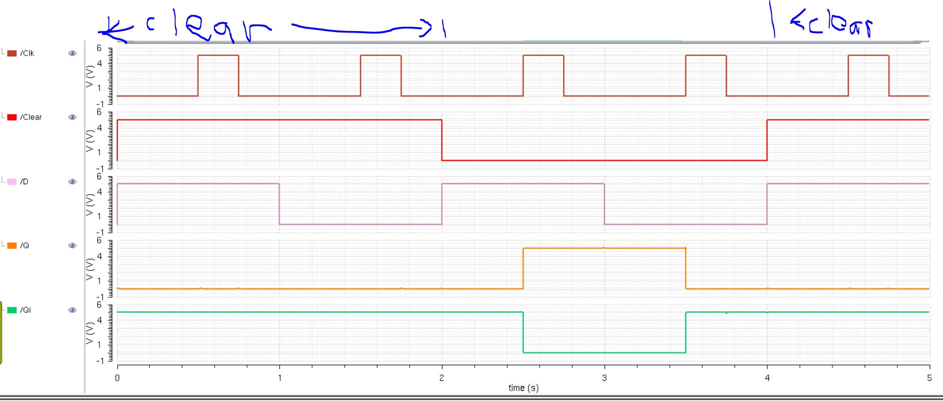
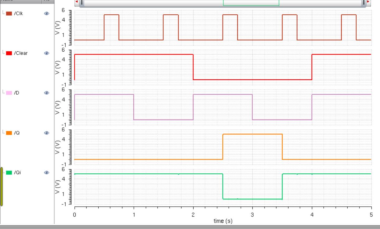
Counting down then clear

Counting up then clear

Extracted UP

Extracted Down

zip
