Project - EE 421L
Authored
by Youssef Abdallah,
abdaly1@unlv.nevada.edu
November 23, 2015
Pre-lab work
- Back-up all of your work from the lab and the course.
- Go through Cadence Tutorial 6 seen here.
- Read through the lab in its entirety before starting to work on it
Lab Report
First
half of the project is the schematics, symbols, and simulations of the design
1) Design of an 8-bit resettable (input "clear") up/down counter
- Design of the D- flip flop used for the counter with clear input and buffered clocked


- Design
of 1-bit D-flip flip with a selector (switch "UP") to count up or
down. If the switch is closed (high) the counter counts up, and if it
is open (low) the counter counts down.


- BUS of 8-bit array
to create an 8-bit counter with clear input. If clear is high the
counter resets and it counts up or down depending on the switch if
clear is low


- The
following simulation shows the function of the counter. At first it
counts UP (switch is closed and clear is low), then clear resets the
count. After, the switch opens, clear goes low, and the counter counts
down


2) A 31-stage ring oscillator with a buffer for driving a 20 pF off-chip load - Design of a 6/6 inverter used to create the 31 ring oscillator


- Design of a buffer to drive a 20 pF load


- The following simulation show the output of the 31 ring oscillator driving a 20 pF load


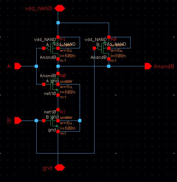
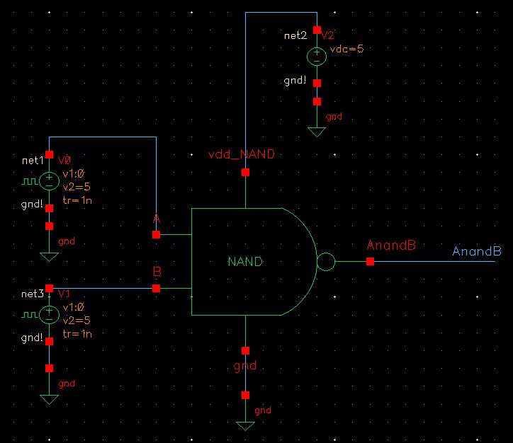
3) NAND and NOR gates using 6/0.6 NMOSs and PMOSs
- NAND gate schematic, symbol, and simulation


- NOR gate schematic, symbol, and simulation


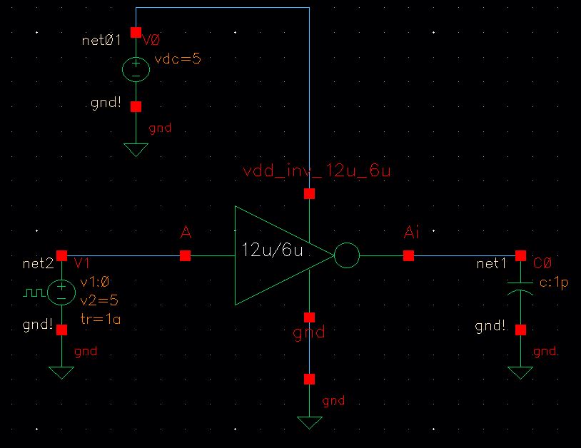
4) An inverter made with a 6/0.6 NMOS and a 12/0.6 PMOS
- 12u/6u Inverter schematic, symbol, and simulation driving a 1pF load


5)
Transistors, both PMOS and NMOS, measuring 6u/0.6u where all 4
terminals of each device are connected to bond pads (7 pads + common
gnd pad)
- 6u/0.6u NMOS schematic, symbol, and simulation. ID vs VDS and ID vs VGS


- 6/0.6 PMOS schematic, symbol, and simulation. ID vs VSD and ID vs VSG


6) A 25k resistor implemented using the n-well (connect between 2 pads but we also need a common gnd pad)
- Schematic, Symbol, and simulation of the output current


7)
Using the 25k resistor laid out below and a 10k resistor implement a
voltage divider (need only 1 more pad above the ones used for the 25k
resistor)
- Schematic, symbol, and simulation showing the result if the input is 5V


- The
final schematic shows the symbol of each circuit and the corresponding
assigned pin for each input and output pad (with common gnd).

The second half of the project is to layout each circuit of the design
- Each layout is DRC clean, has been LVSed, and it show that the netlists match
1) Layout of an 8-bit resettable (input "clear") up/down counter
- Layout of the D- flip flop used for the counter with clear input and buffered clocked


- Layout of 1-bit D-flip flip with a selector (switch "UP") to count up or
down. If the switch is closed (high) the counter counts up, and if it
is open (low) the counter counts down.


- Layout of BUS of 8-bit array
to create an 8-bit counter with clear input. If clear is high the
counter resets and it counts up or down depending on the switch if
clear is low


2) Layout of a 31-stage ring oscillator with a buffer for driving a 20 pF off-chip load - Layout of a 6/6 inverter used to create the 31 ring oscillator


- Layout of a buffer to drive a 20 pF load


- Layout of a 31-stage ring oscillator


3) Layout of NAND and NOR gates using 6/0.6 NMOSs and PMOSs


4) Layout of an inverter made with a 6/0.6 NMOS and a 12/0.6 PMOS


5)
Layout of Transistors, both PMOS and NMOS, measuring 6u/0.6u where all 4
terminals of each device are connected to bond pads (7 pads + common
gnd pad)


6) Layout of a 25k resistor implemented using the n-well (connect between 2 pads but we also need a common gnd pad)


7) Layout of the
voltage divider (need only 1 more pad above the ones used for the 25k
resistor)


- The project design directory could be downloaded from the following link project.zip
All the work has been saved and backed up to Google Drive

Return to EE 421L Labs