Lab 06 - ECE 421L
Authored
by Worku, Yetneberk
Email: workuy@unlv.nevada.edu
NHSE ID 1007208058
10/17/2014
Pre-Lab six
Back-up all of your work, and go through cadence tutorial 4
Post lab 6
the purpose of this lab is to design, layouot, and simulation of a cmos nand gate, xorgate, and full-adder.
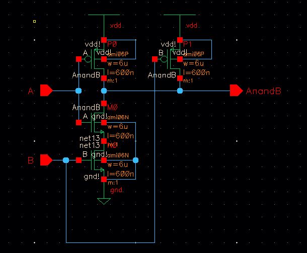
first, copy the files in lab5 to lab6, and create a nand gate then use the mosfets (both nmos and pmos) value to 6u/0.6u.
now,
use those nmos and pmos again then by instances and wire it up as seen
image below, finally, add one more input name it B, and change the
output to AnandB see the image below.
next,
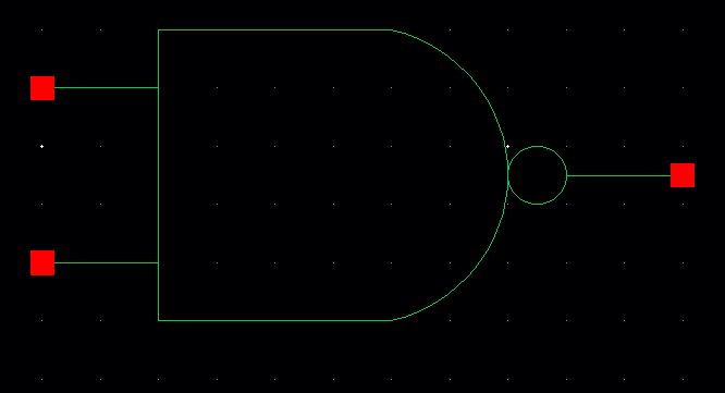
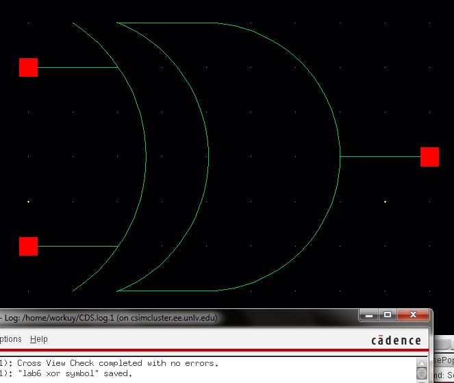
create the nand symbol bye doing
create---->>cellview--->>from cellview; the created symbol
see the image below.
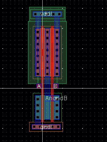
next, create the layout of the component, by modified the inverter form the previous lab,
then delete metal1 and contacts between the two nmos. add metal1 to
gnd!, vdd!, and connect the drains to the two pmos to the drain of the
nmos. also, add a pin to output name it AnandB, and see final layout the image below.
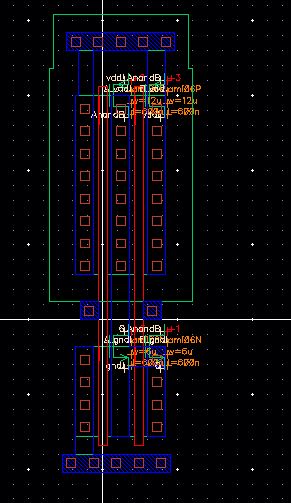
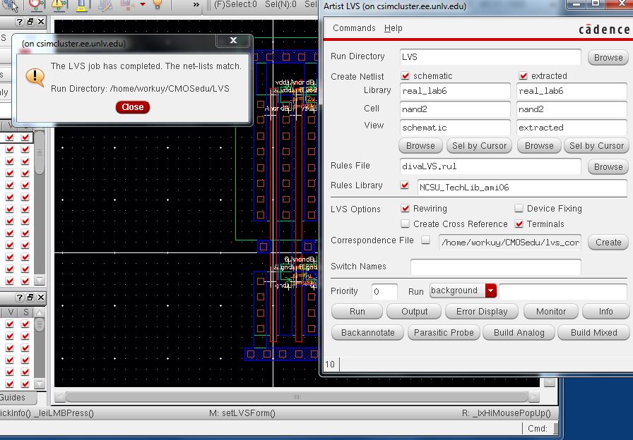
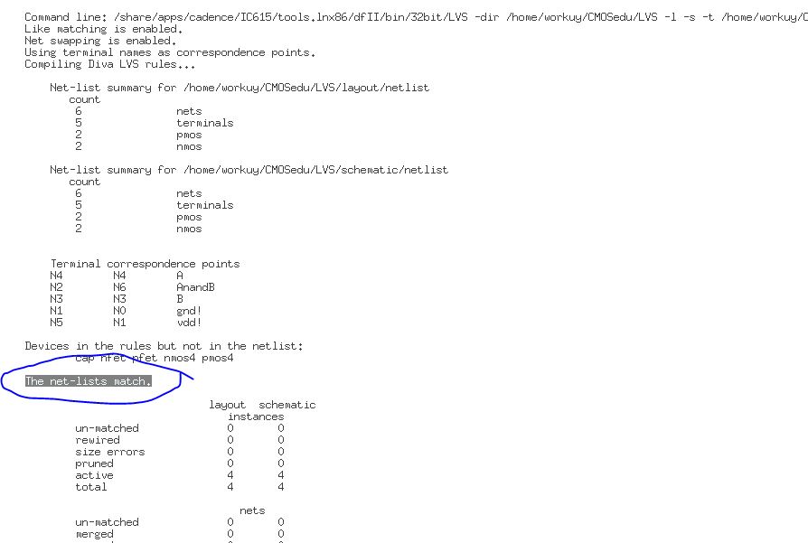
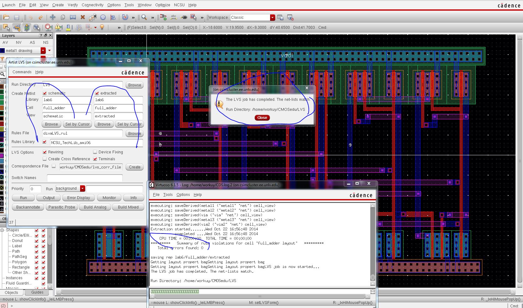
next, extracting and lvs. see the result image below
next,
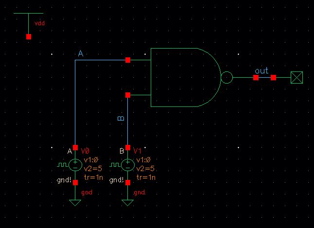
simulate the NAND gate, by createing a new cell view schematic for the
simulation. i have chosen 20ns and 40ns periods. see the schematic
image below.
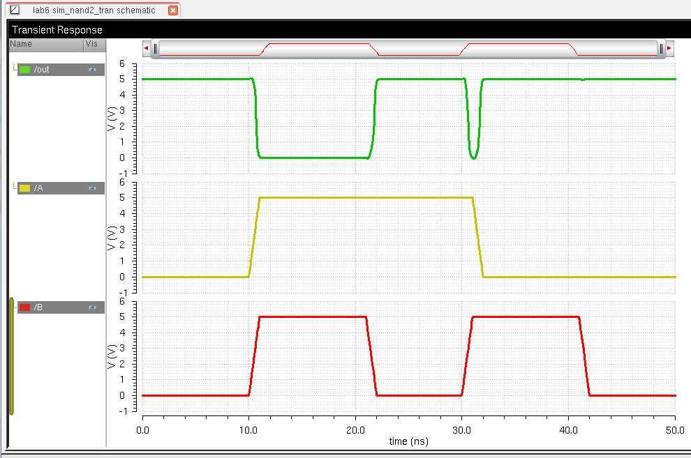
next, create a new cell view schematic for the simulation nand gate, see the image below
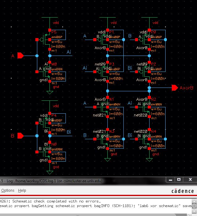
Second, create xor gate
next, the check and save; completed schematic image showing below
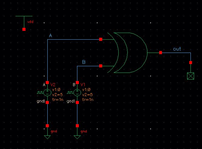
next, simulate the XOR gate, by createing a new cell view schematic for the simulation. see the image below.
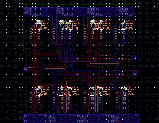
next, create the layout for xor, then check DRC. completed layout see the image below.
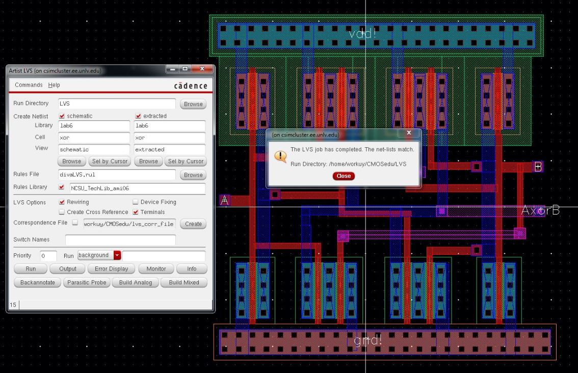
next, extract the layout and lvs it with the schematic, that must be much. see image below.
next,
time to create nand and xor gate. the nand and xor designed similar to
the schematic; also, the simulation result the image showing below.
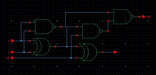
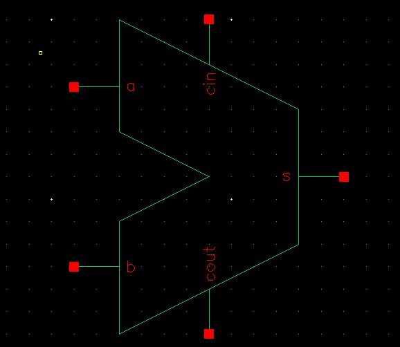
next,
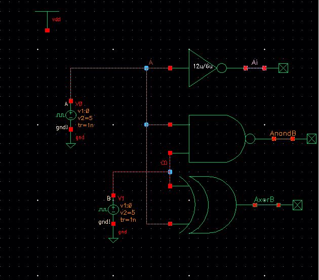
creating the full adder. we have the nand and xor gates, so see the
completed schematic, and symbol of the full adder showing below.
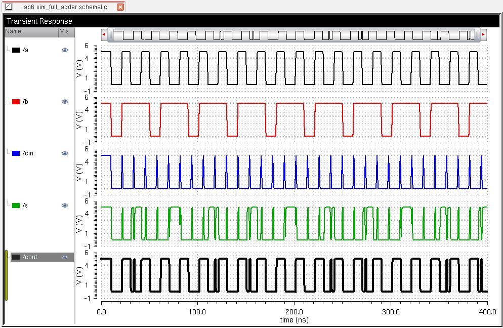
next, now we sumulate full addeer, the following truth table will our reference
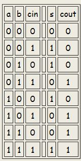
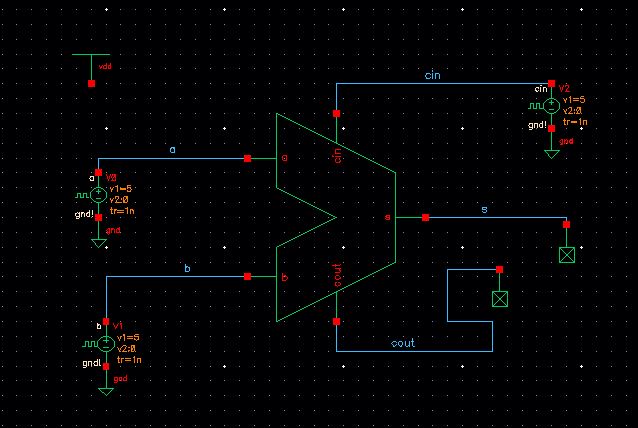
next,
based on the tuth table we will have three voltage sources for a, b,
cin inputs. cin is output, and s is sum. here is the simulation
schematic showing below
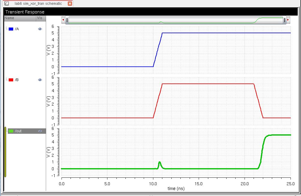
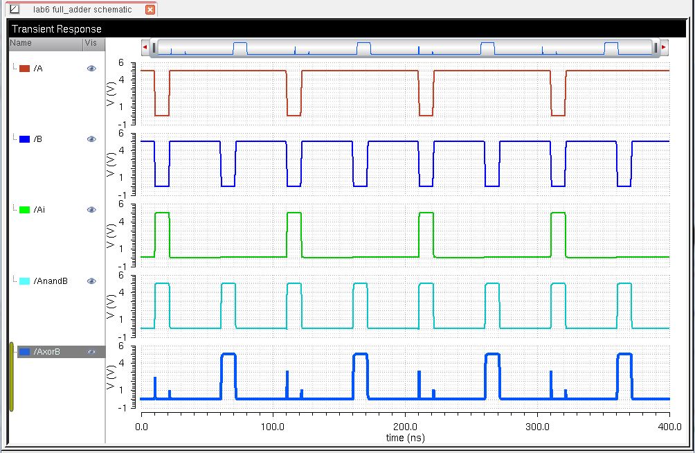
next, the simulation results as seen below.
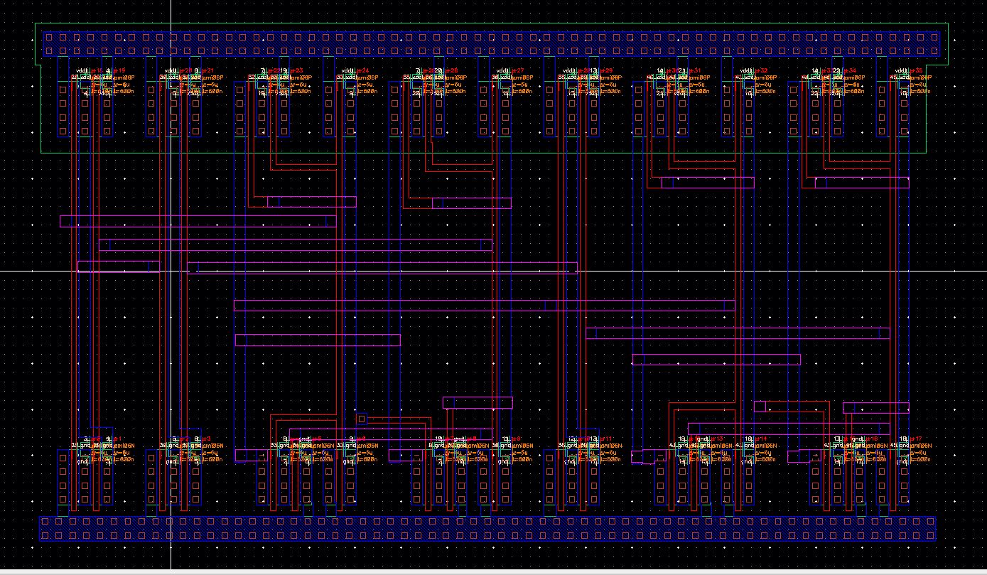
next, for layout can use the xor and nand gate.
finally,
comment about this lab i notice in the plot of the image output not
perfectly square pulses, because there are delays for each gate.
Add
a return to the listing of your labs
backup my work, i e-mail it my self

the lab6 download is here
Return to the listing of my labs
Return to the whole class report
Return to the EE421L site
Return to the CMOSedu.com