Lab
X - ECE 421L
Authored
by Worku, Yetneberk
Email: workuy@unlv.nevada.edu
NHSE ID 1007208058
10/08/2014
Pre-Lab five
Before we get going with this tutorial please make sure you know the answers to the following questions.
If you don’t, or the answers don’t come to you quickly, then go back through Tutorial_1 and Tutorial_2
1.What does the Bindkey q do?
will select object and open the properties; what we selected.
2. Which two Cell Views are used when doing an LVS?
Schematic view and Extracted view.
3. What is the difference between the nmos and nmos4 schematic cells?
nmos tied to ground
4. How do you select the MOSFET models in the ADE window? What does ADE stand for?
select setup>>>model libraries and ADE stand for Analog Design Environment
5. What is the difference between moving and stretching?
moving means moving the object new place, but
stretching means making the object; we select
extended or make it biger or small.
6. How do you layout a rectangle on the metal1 layer?
first, select the metal layer then press R.
7. What does the ! indicate at the end of gnd! and vdd!
it is a global variable.
8. What do the acronyms LSW and CIW stand for?
layer selection window, and commond intrperter window.
9. How is the ruler used? Cleared?
press K, shift + K
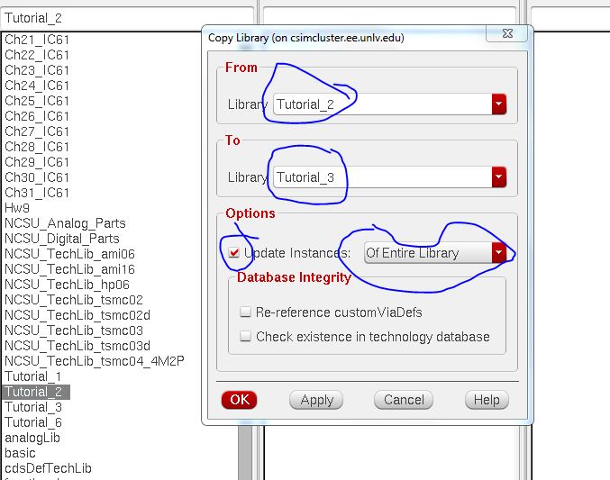
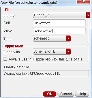
Now,
assuming Virtuoso has been started in the CMOSedu directory, by copying
the Tutorial_2 library to a library named Tutorial_3, and create a
schematic cell view calledc inverter. see image below
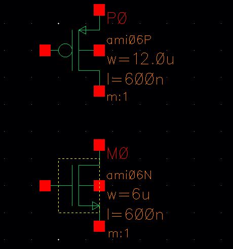
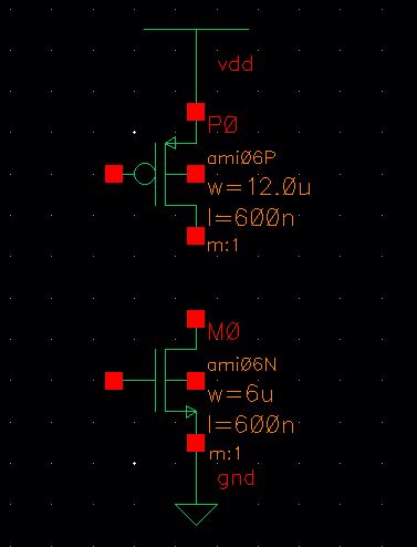
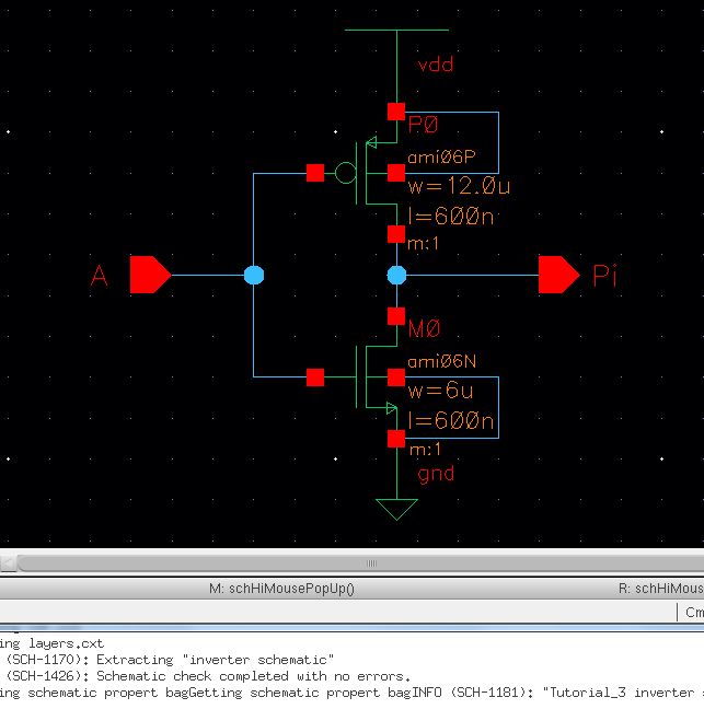
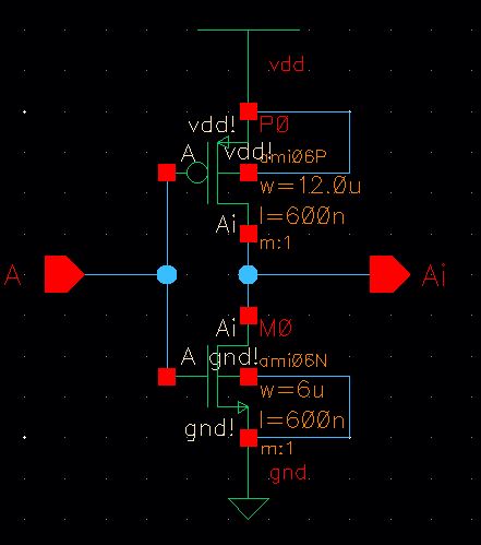
With
this new schematic view open also open the schematic view of NMOS_IV,
and Pmos_IV window get the following image below, aslo instantiate vdd
and gnd supply nets, the main time wire up the inverter, add pins and
cheak save as seen below.
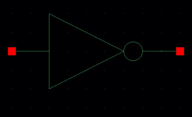
next,
create the symbol for the inverter, delete everything in the inverter's
symbol, create the layout view for the inverter. check and save see
image below
next,
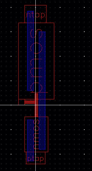
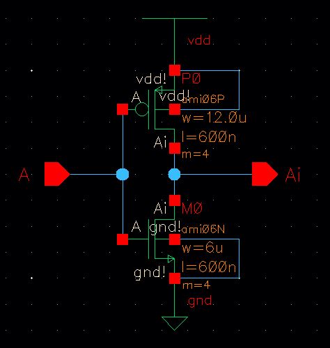
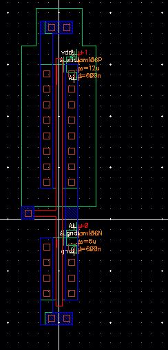
add the folloing cells such as nmos, pmos, ntap, ptap, and m1_poly.
also, make sure nmos is 6um width, and pmos is 12um width; add
rectangles on ply and metal1, finally cheac and save as seen the image
below.
next,
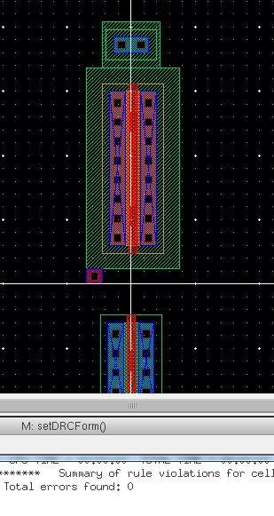
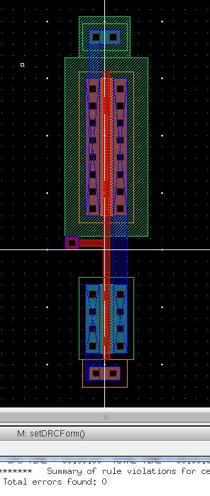
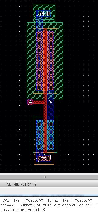
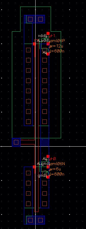
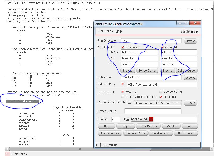
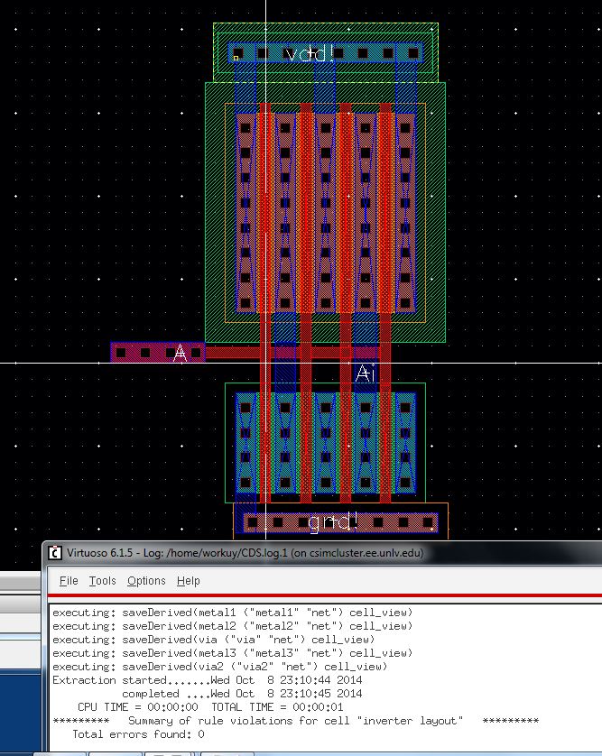
add pins on metal1 for gnd!, vdd! name it input (A), output (Ai). drc
and save the sesign. then run extraction on the layout, and finally run
the LVS on the inverter see image below
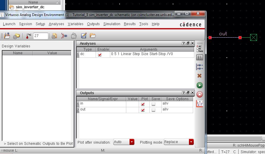
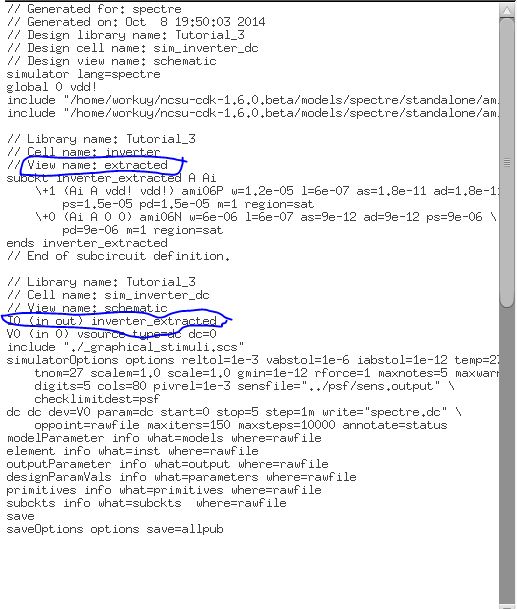
now,
create a cell called sim_inverter_dc draft the folloing schematic, and
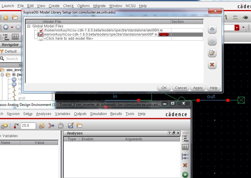
start the ADE . then setup--> modellibraries. next select analyses,
plotted, and save the state in thelcellview save and cheak; see the
image below
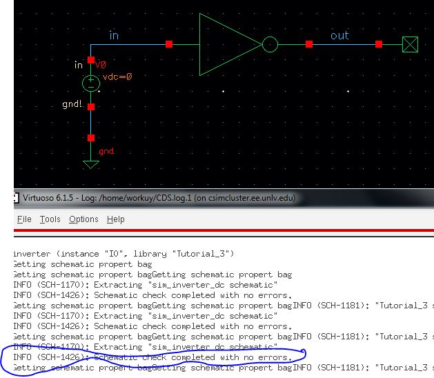
next, netlist and run the simulation the results seen image below
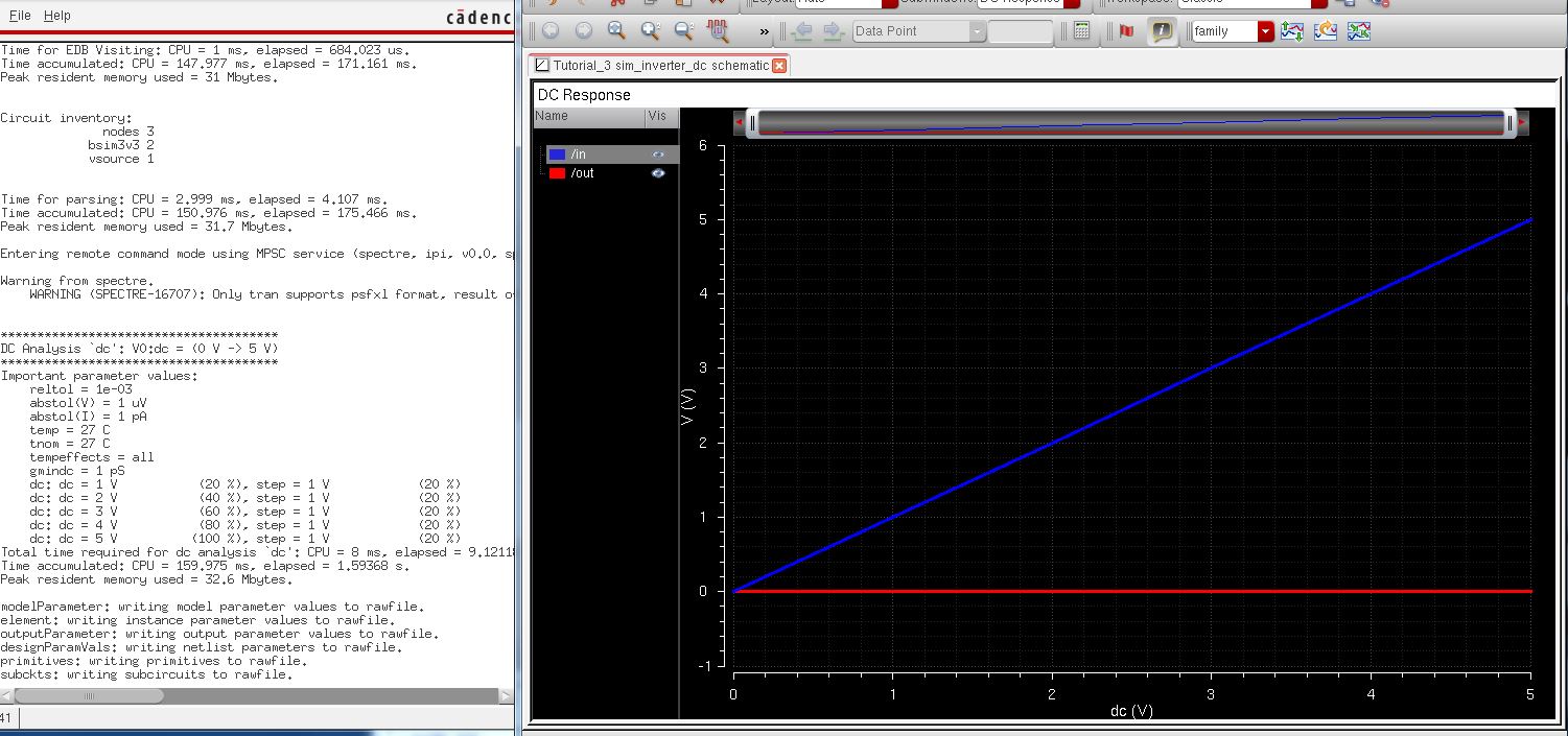
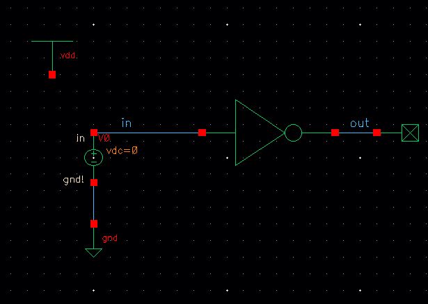
we did't specify a vdd! anywher so it should be zero let fix the issue. to fixe let's add vdd symbol as seen below
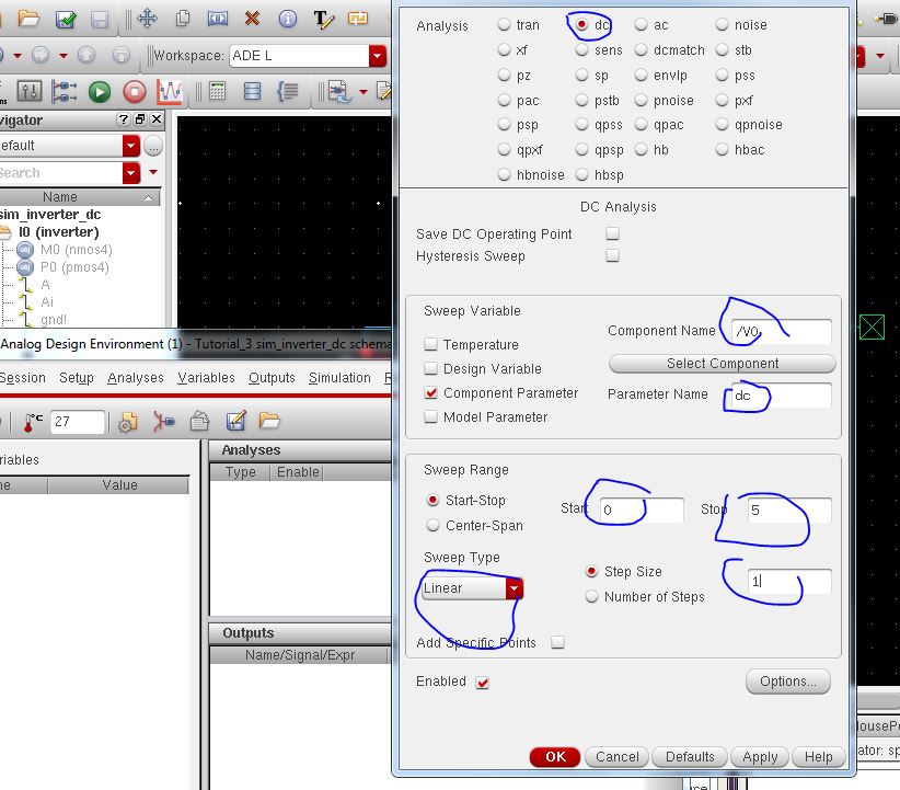
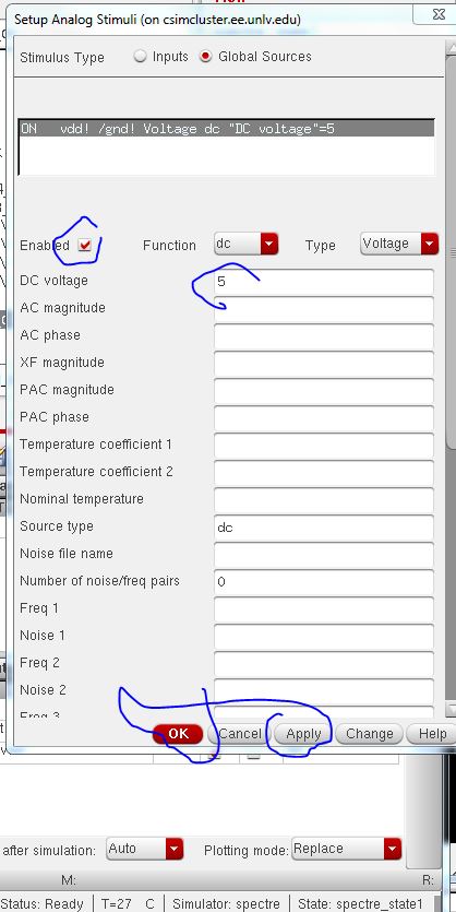
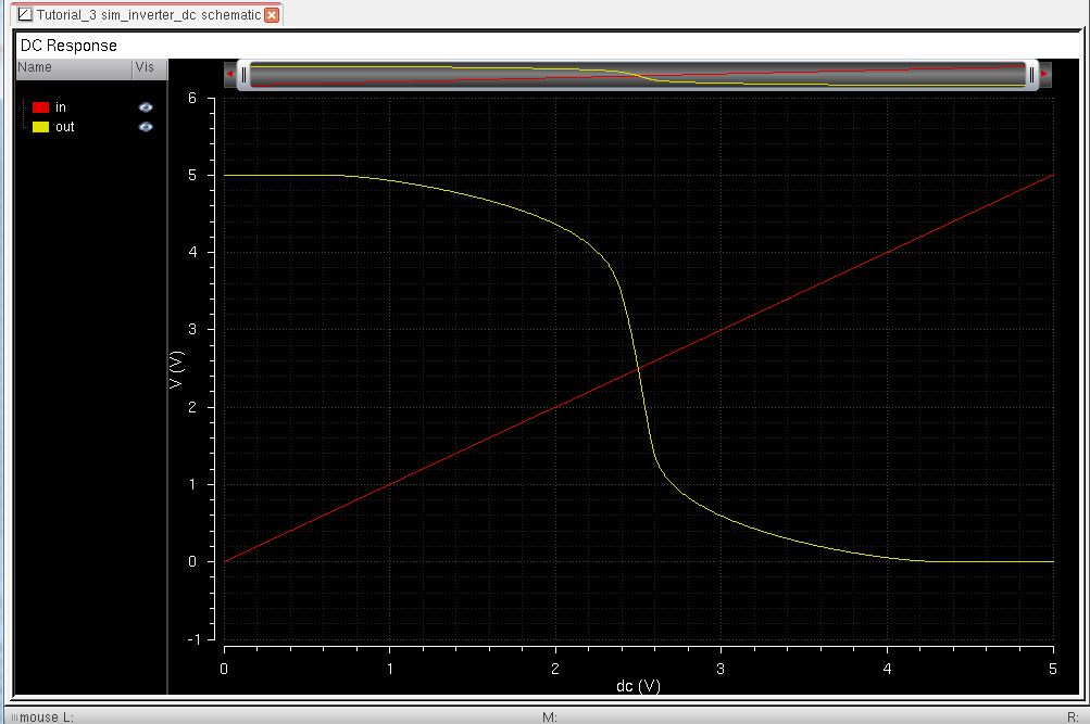
next,
in the ADE select setup-->stimuli and the parametrs seen below, also
the results are the inverter voltage transfer curves to look like the
following image.
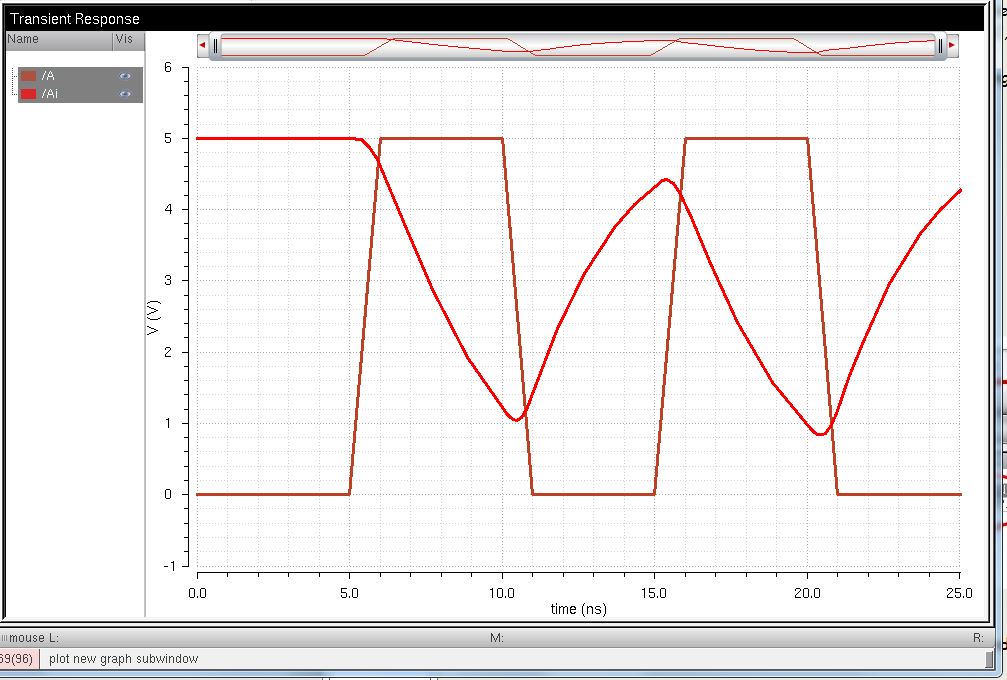
now, simulate the extracted layout the reslut below
post lab
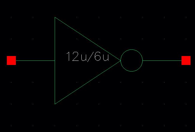
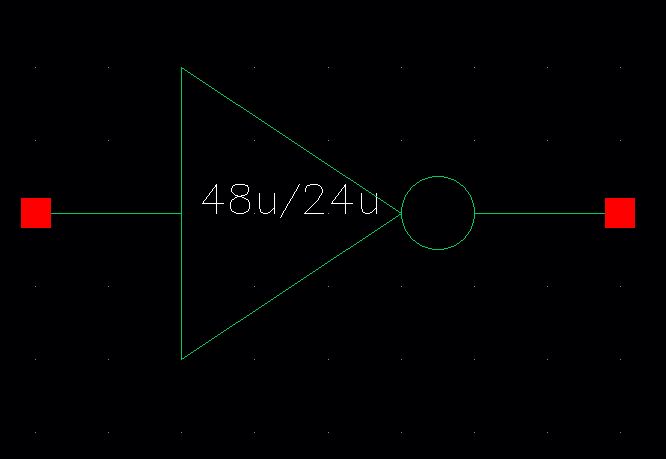
In this lab copy the previous inverter, rename as 12u by 6u pmos and nmos respectively, so see the folloing image show that
next, the created symbols for the two inverters with 12u/6u and 48u/24u the image showing below
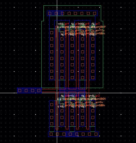
now,open the layout view and change the multiplier to 4, for both the PMOS
and NMOS Next increase the size of the ntap and ptap. see image below
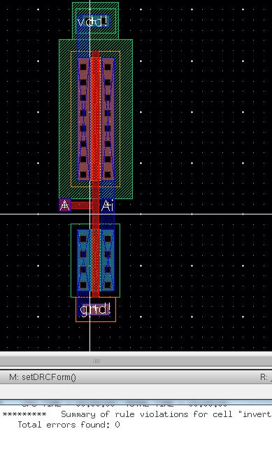
Next, the extracted views form layouts see the following images
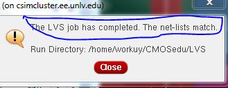
next, time to cheak both transistors and lvs checked that the see the result image beow
 Now,
using spice simulate the oeration of both of your inverters shoing each
driving a 100pF,10pF, and 100pF capacitive load. the following image
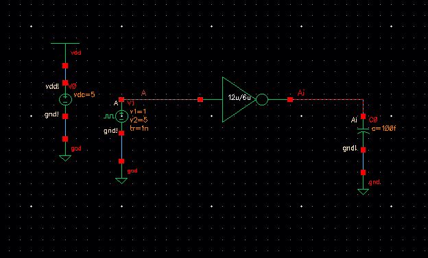
show the schematic of 12u/6u inverter.
Now,
using spice simulate the oeration of both of your inverters shoing each
driving a 100pF,10pF, and 100pF capacitive load. the following image
show the schematic of 12u/6u inverter.
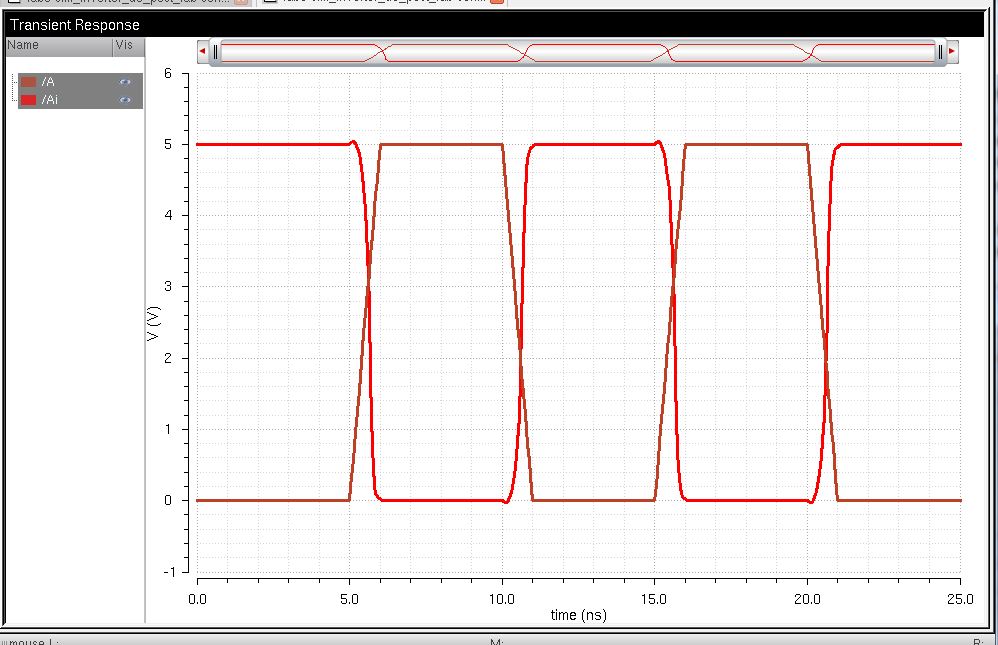
next, the 12u/6u inverteris driving a 100fF capacitor
 next, the 12u/6u inverteris driving a 1pF capacitor
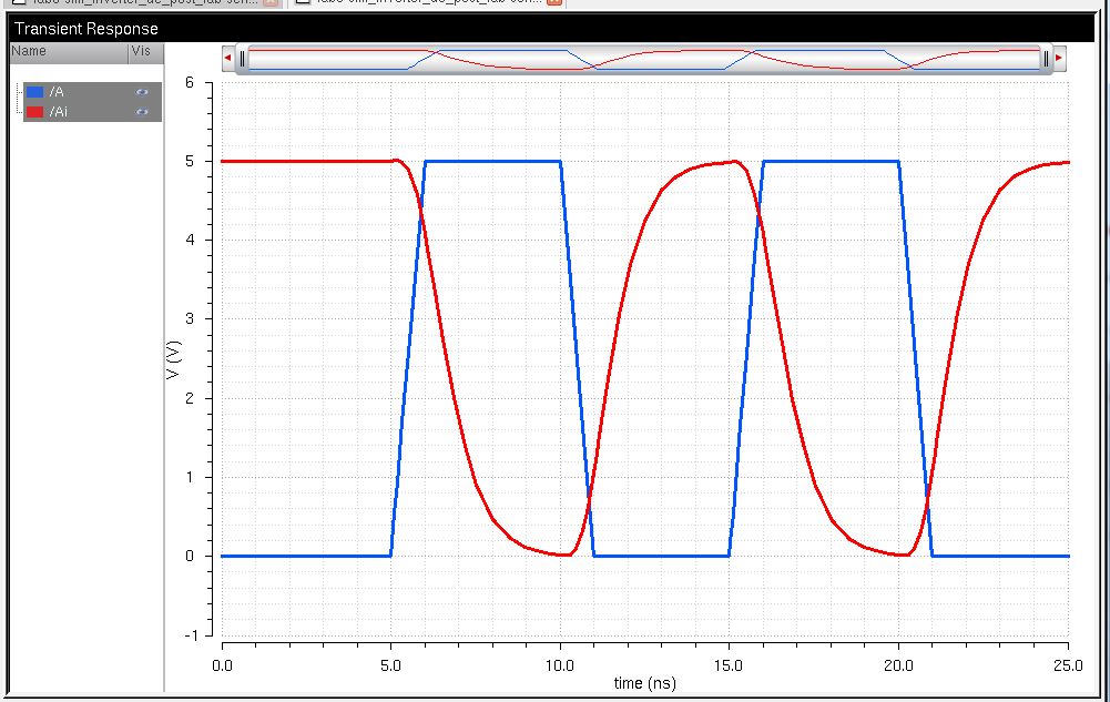
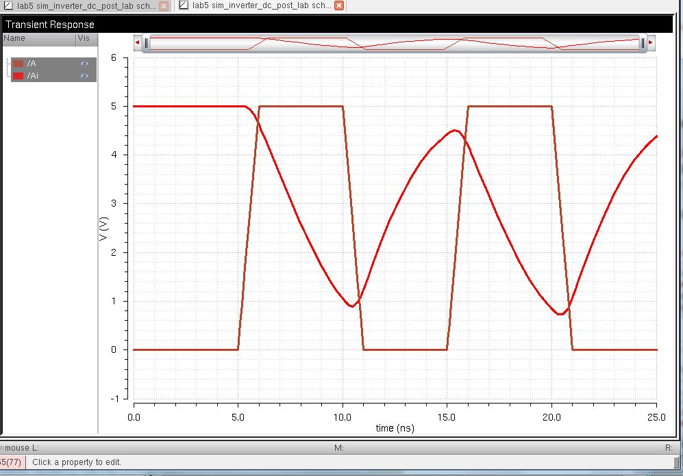
next, the 12u/6u inverteris driving a 100pF capacitor
the comment i have by increasing the volue of capacitor, the inverter have limitation becauser of capacitance.
next, schematic of 12u/6u inverter. see the image below
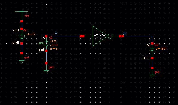
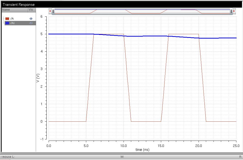
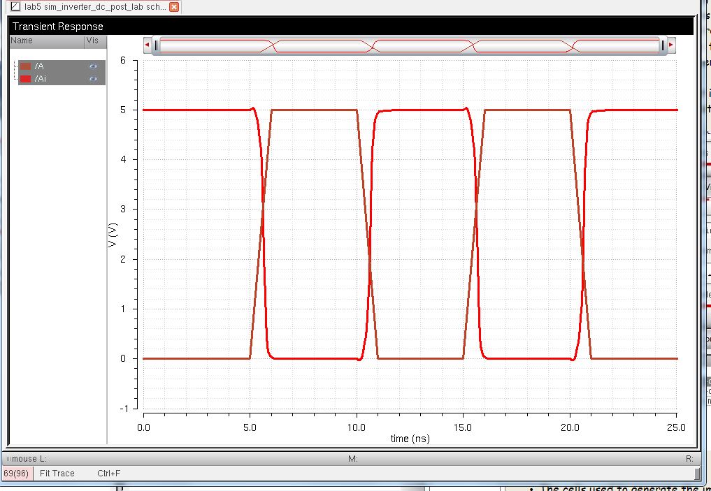
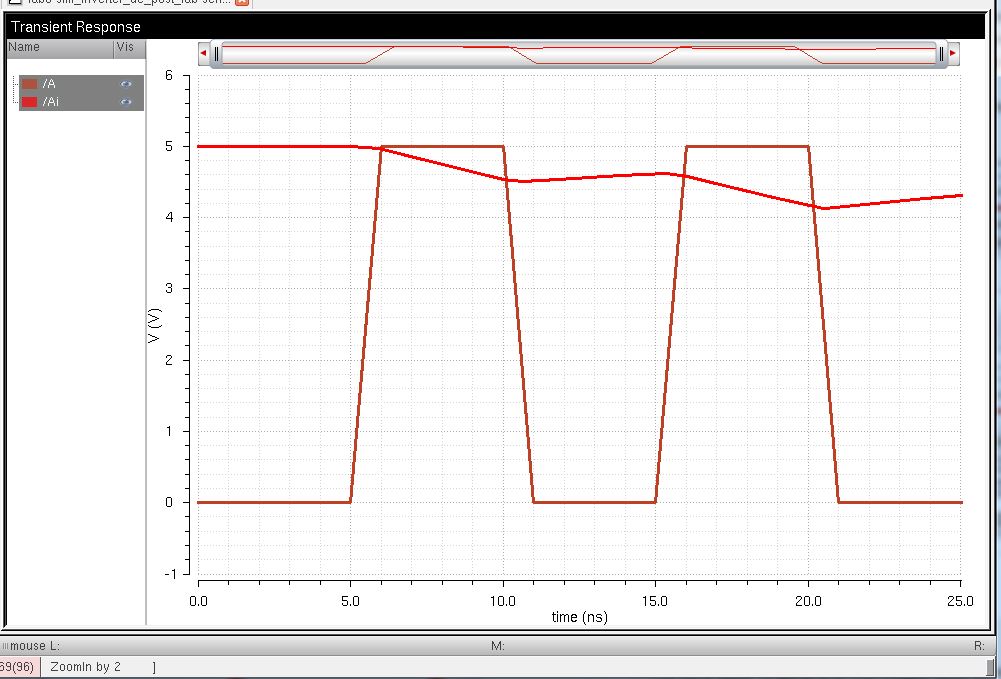
next, the 48u/24u inverteris driving a 100fF capacitor
next, the 48u/24u inverteris driving a 10pF capacitor
next, the 48u/24u inverteris driving a 100pF capacitor
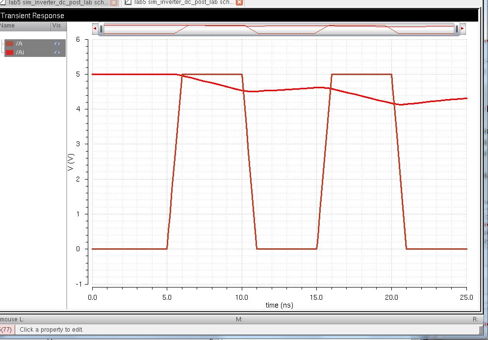
comment i have or i observe is by increasing the volue of capacitor, the inverter have limitation becauser of capacitance.
next now doing with Ultrasim to do that we sued setup-->simulator/directorty/host and select ultrasim as seen below
next, the 48u/24u inverteris driving a 100fF capacitor
next, the 48u/24u inverteris driving a 10pF capacitor
next, the 48u/24u inverteris driving a 100pF capacitor
Finally,
there is no different between ultrasim simulation and spice
simulation, however, bigger inverters will have higher multipliers can
handle larger capacitance.
backup the work

Add
a return to the listing of your labs
the lab5 download is here
Return to the listing of my labs
Return to the whole class report
Return to the EE421L site
Return to the CMOSedu.com