Lab
X - ECE 421L
Authored
by Worku, Yetneberk
Email: workuy@unlv.nevada.edu
NHSE ID 1007208058
09/29/2014
Pre-Lab four
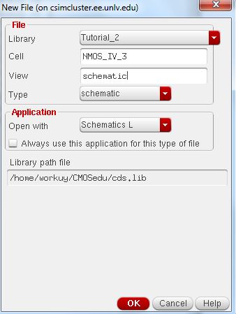
1. back up all of the work from the lab and the course and read through lab and see Totorial 2.
2.
make shure the simulations in this lab the body of all NMOS devices
(the substrate) should be at ground and the body of all PMOS devices
(the n-well) should be at a vdd of 5V.
Post-lab four
The purpose of this lab is both the NMOS and PMOS I-V characteristics of simulations.
Now,
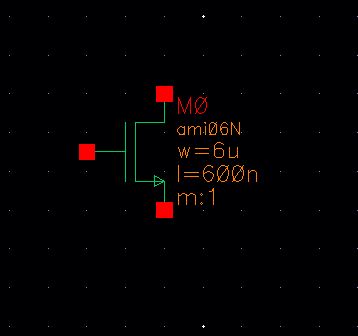
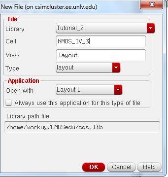
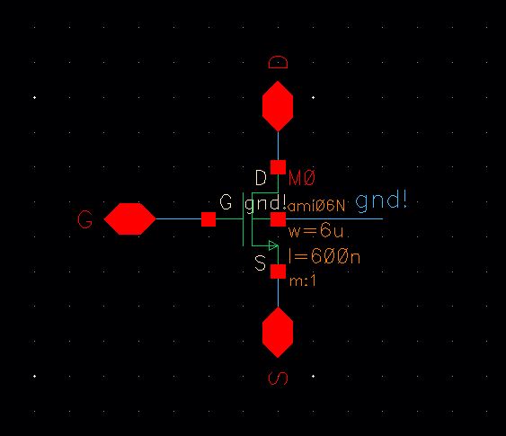
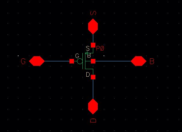
creating a schematic cell called NMOS_IV_3 as seen below, 3 indicates
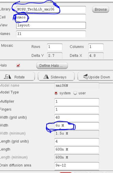
I'will use a 3 terminal transistor. press i then set the transistors
width to 6um and length at 600nm.
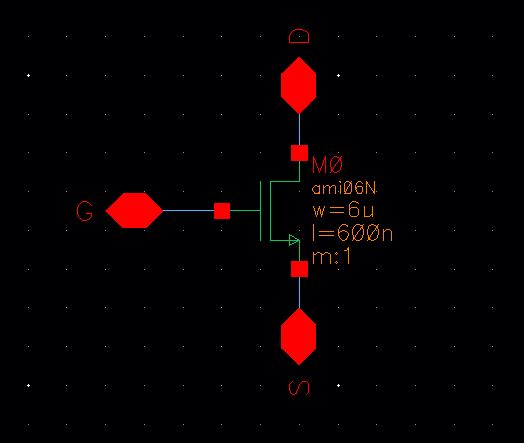
next, adding pins with direction as seen below.
next,
creating a symbol view for this schematic, delete everything in the
cell except the pin, then draw a MOSFET symbol; the images showing below
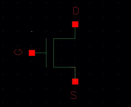
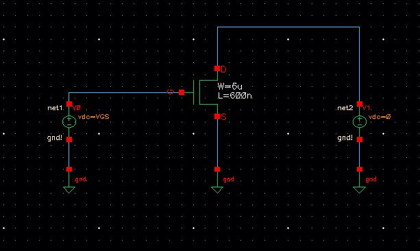
next,
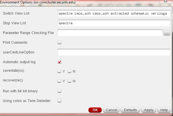
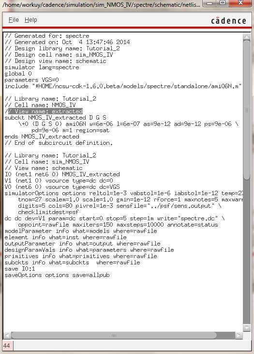
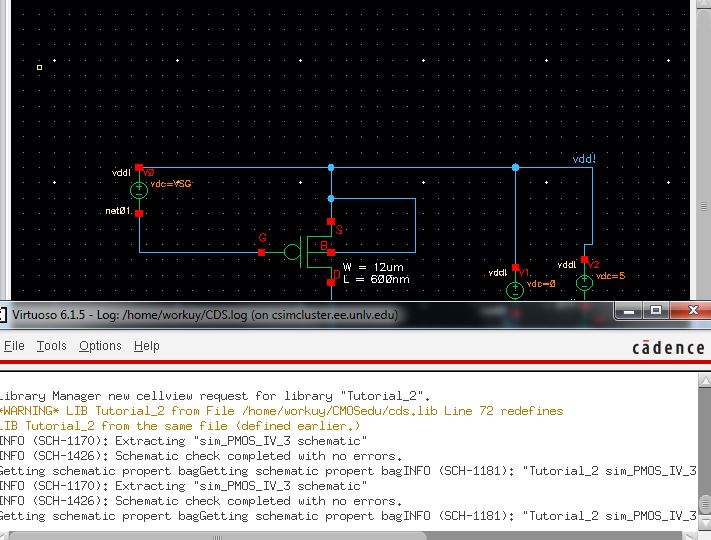
create the NMOS_IV_cell view and the dc voltage sources seen below,
also wire things up and save cheak. then Launch the ADE, then go to the
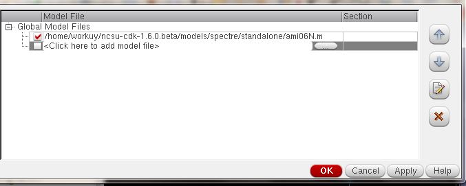
menu setup--> model libraries, select, and set
ncsu-cdk-1.6.0.beta/models/spectre/standalone/ami06N.m , seen the image
below.
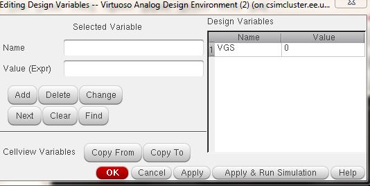
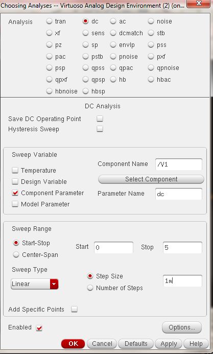
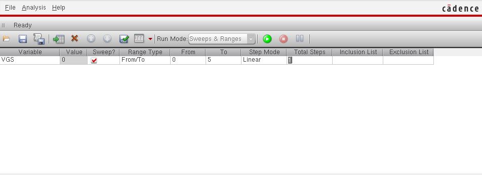
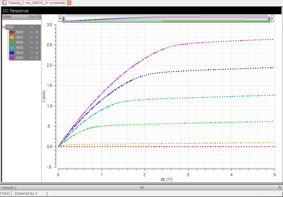
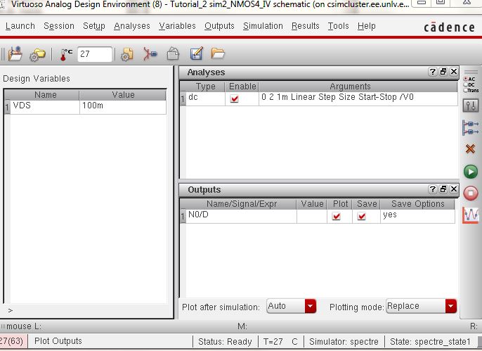
next, add VGS, and choose set the parameters seen below.
next,
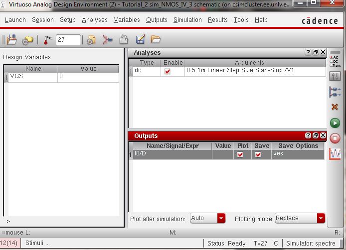
clicking on the D pin the select the current. both plotted and
saved are selected, also set parameters; seen the image below.
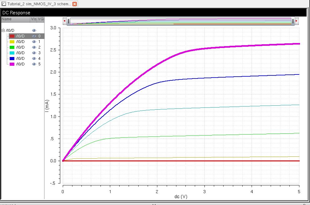
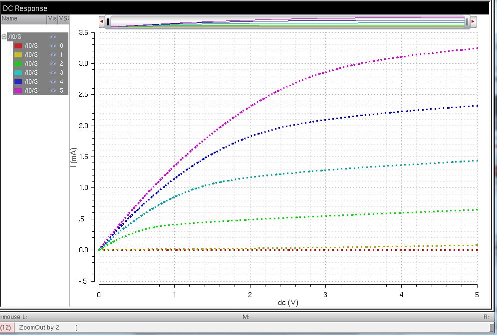
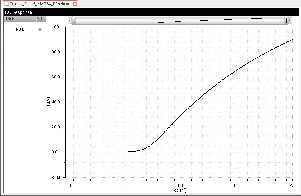
Finally, run analysis then see the MOSFET IV curves below.
stop the ADE and save the state then close all cell views.
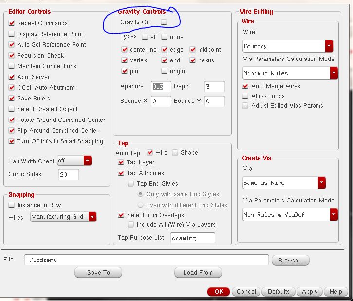
we are now ready to create a layout view for NMOS_IV_3, and to edit gravity controls. see fig below.
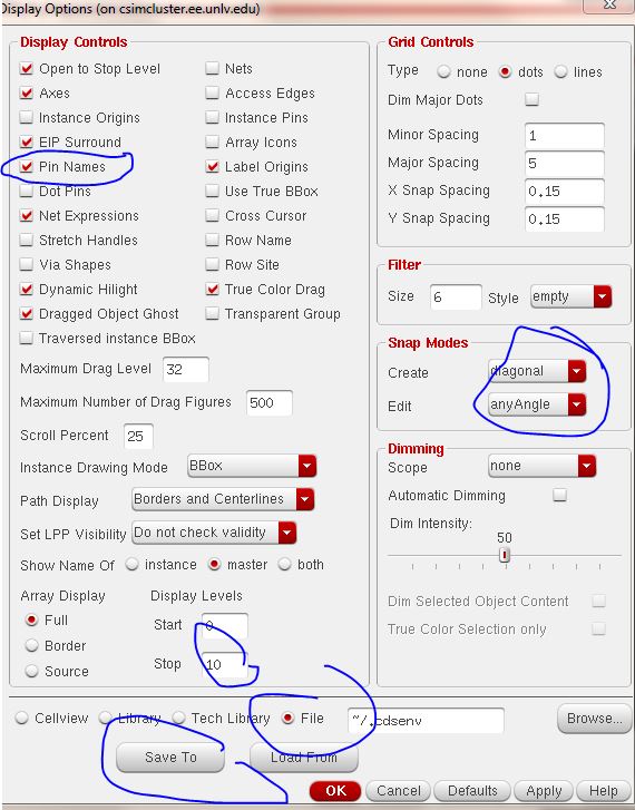
next, make sure pin names, snap modes,file, stop (10), and save to selected. see image below
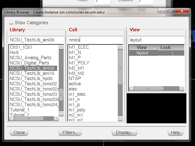
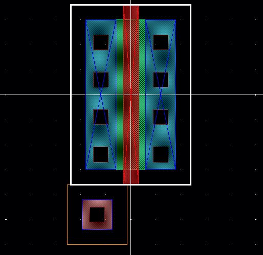
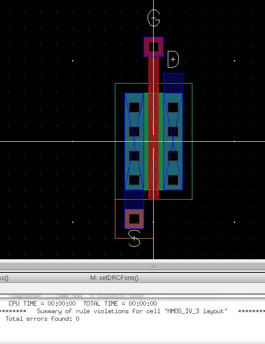
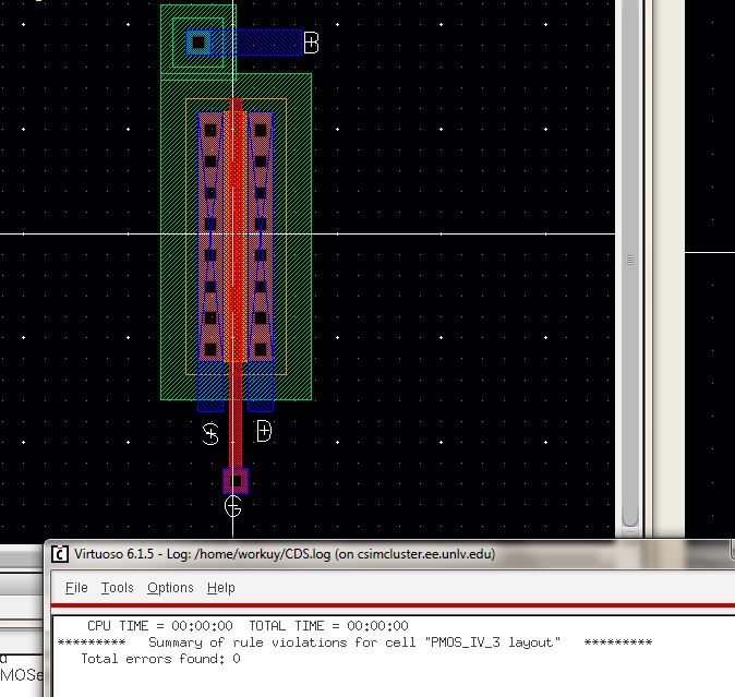
next instantiate an nmos device that is W=6um, and L=600nm long. seen fig below
next,
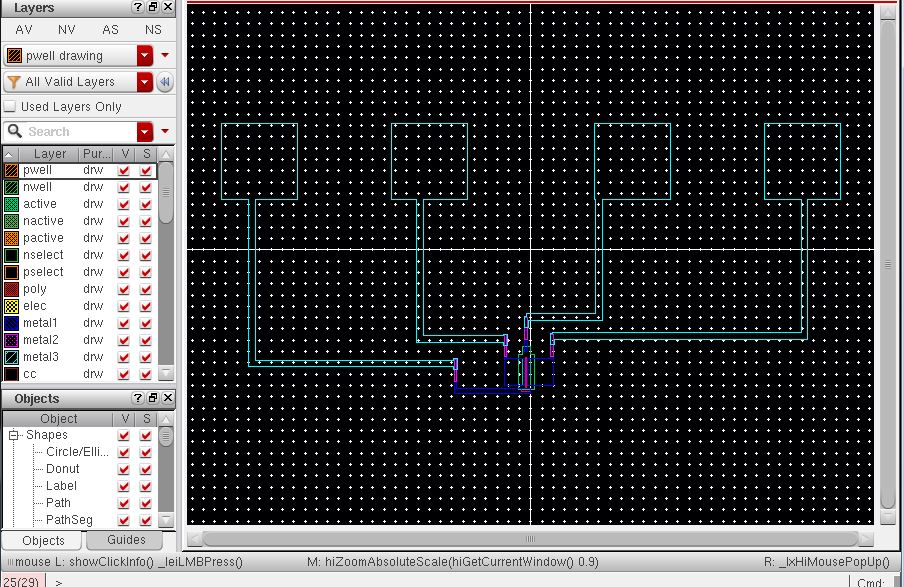
instantiate a ptap cell, and add metal1 layer to connect the source to
the p-substrate and the drain. also, add metal1 connection to poly
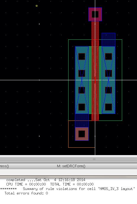
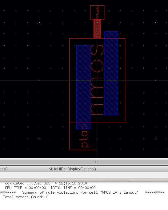
cell, then alwayes cheak DRC layout. seen the image below.
next
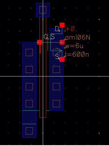
by pressing e and then select stop to 0; we can see the rectangles and
cell. also see it back what it was. then label the pin. always cheak
see image below.
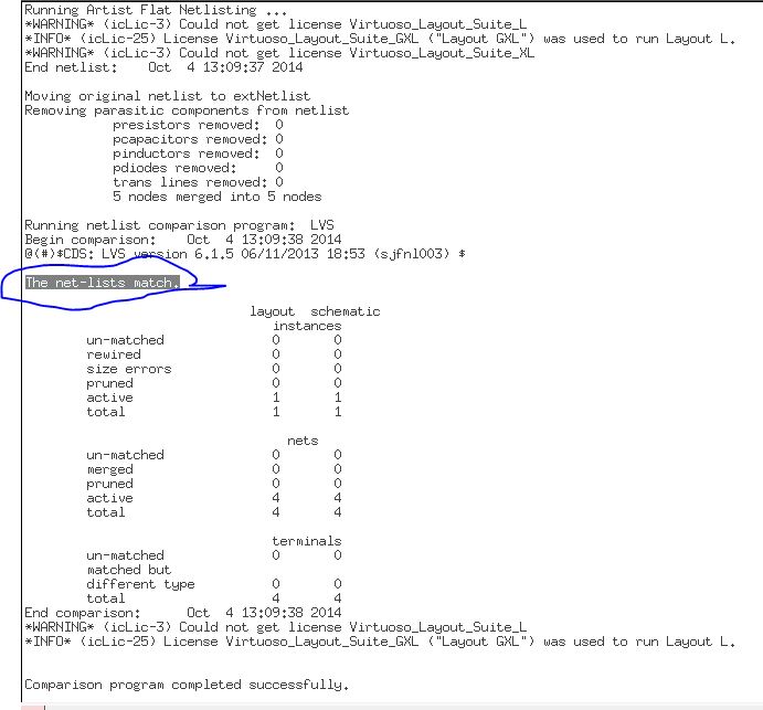
next,
Extract the layout, this LVS will run error, because the 3 terminal
mosfet symbol is used. however, see the image below, but is going to be
fixed.
next,
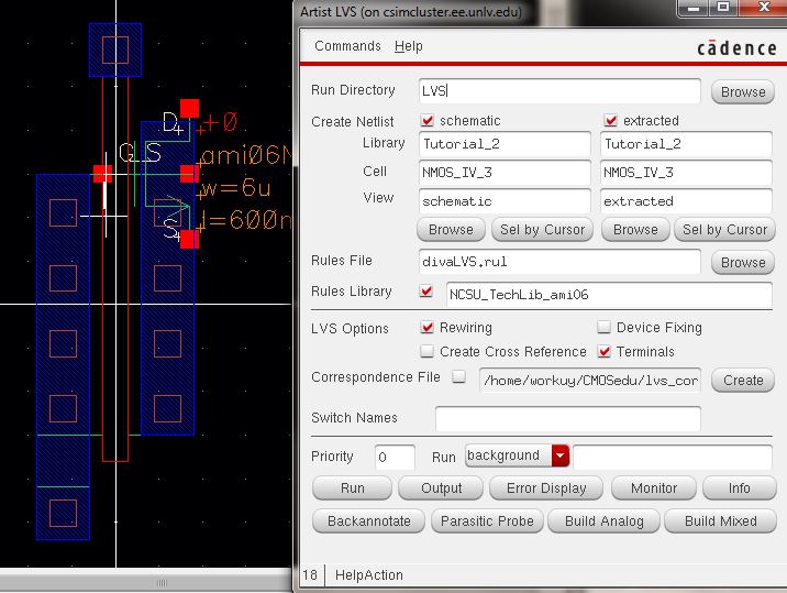
let fix the problam close all cell views. open the liberay manager and
rename NMOS_IV_3 to NMOS_IV, the open schematic view of NMOS_IV, then wire it up; then perform an LVS. seen image below

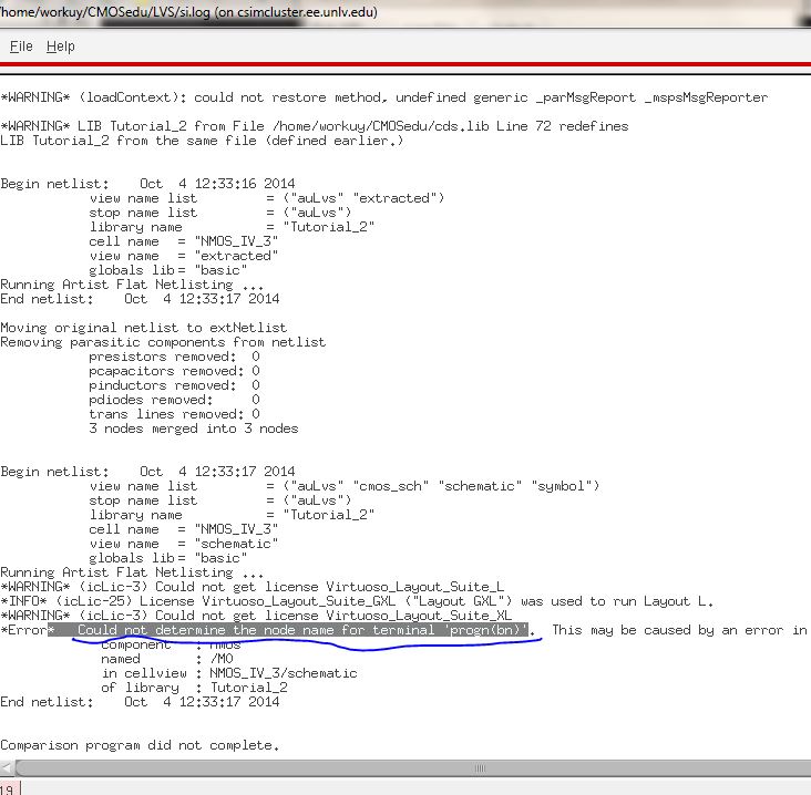
next, run it. if no error will get the net-list match that similar to the image below, also simulate the extracted layout
next, start to simulate as before then will get the result seen below
next simulating the extracted view, the result showing below
now. we are repeating for the same step as NMOS to PMOS divice.
next,
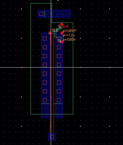
create schematic cell view called PMOS_ID_3 with 4 pins as seen below.
W=12um, and L=600nm. also, save and check, then create a symbol,
pin, layout pmos cell and ntap see image below
next extract the layout, then create a cell and the schematic see the image below
next, the same step as before then only change is not VGS, it is VSG see image below
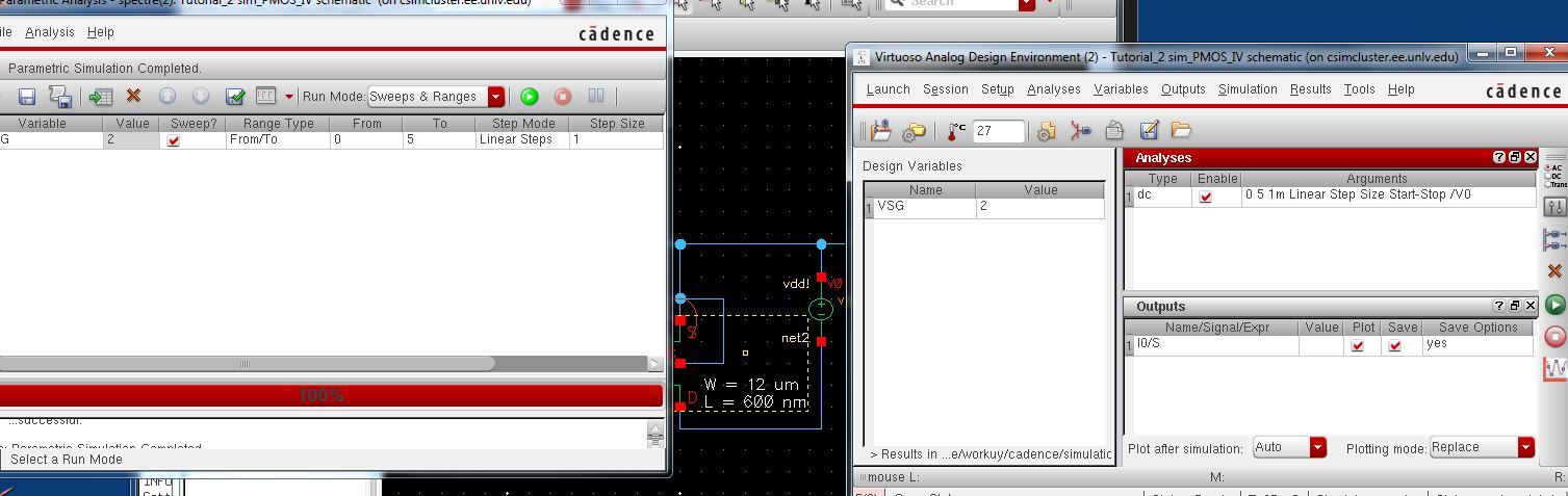
next, starting analysis results see the following image
next, Extracted layout the same result we get see image below
.
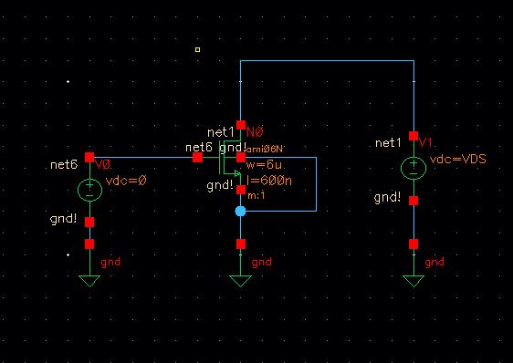
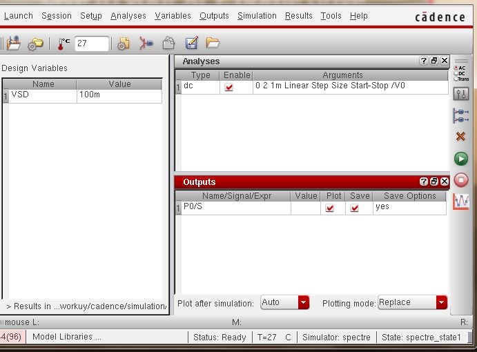
Next, before
exiting save current state; copy the file and replace nmos with nmos4,
then will be plotting ID vs VGS with vds=100mV , vgs will be 0 to 2V in
1mV steps, and keep W=6um, L=600nm. the result image showing below
Next,
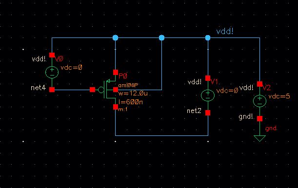
repeat the process for the PMOS copy nmos4 to pmos3. then open
the schematic, chang vgs to vsg add one more voltage with 5V. also,
change the nmos to pmos with set of W=12um and L=600nm. the result see
the image below.
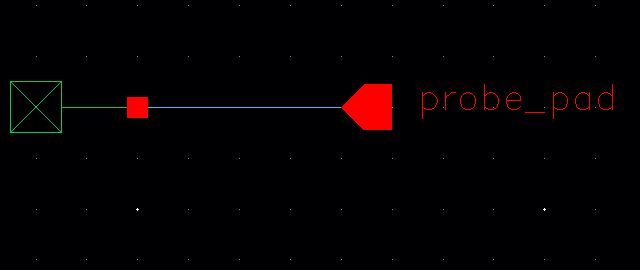
next creating probe pads
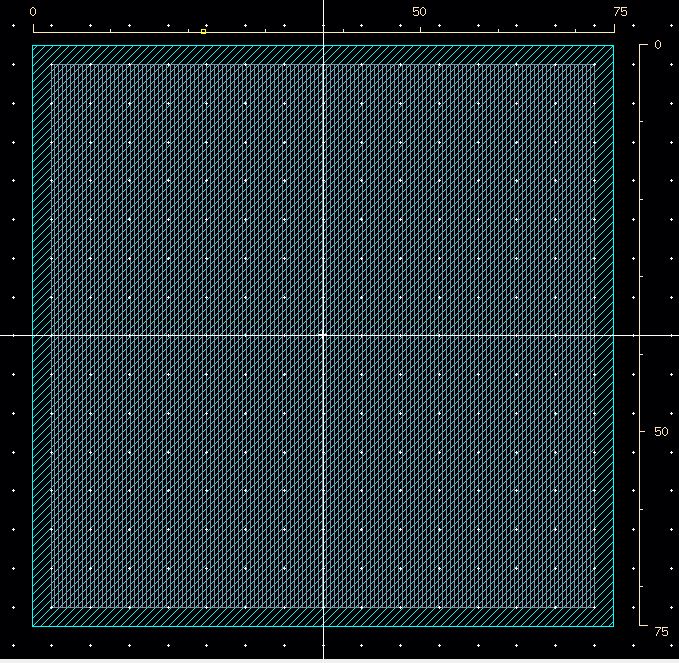
next, create cell view 75um square m3 70un square over glass see image below.
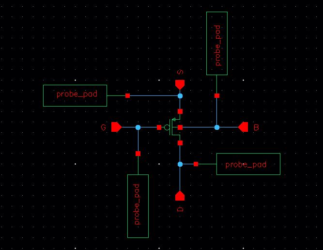
creating a schematic for a 4pin nmos wiht probes
backup
Add
a return to the listing of your labs
the lab4 download is here
Return to the listing of my labs
Return to the whole class report
Return to the EE421L site
Return to the CMOSedu.com