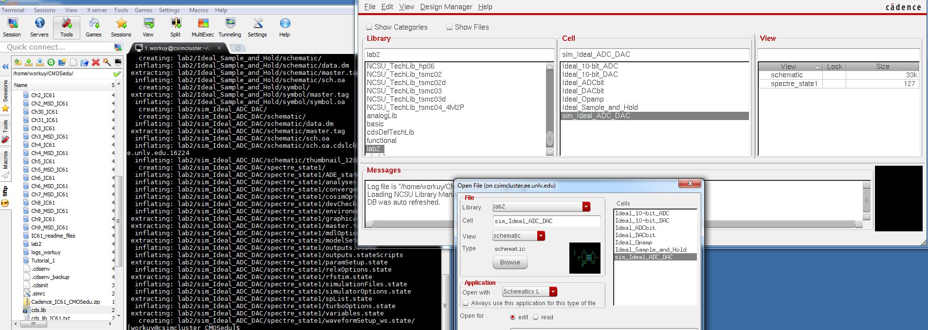
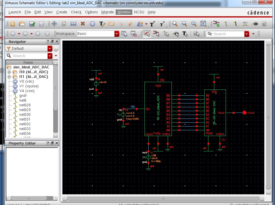
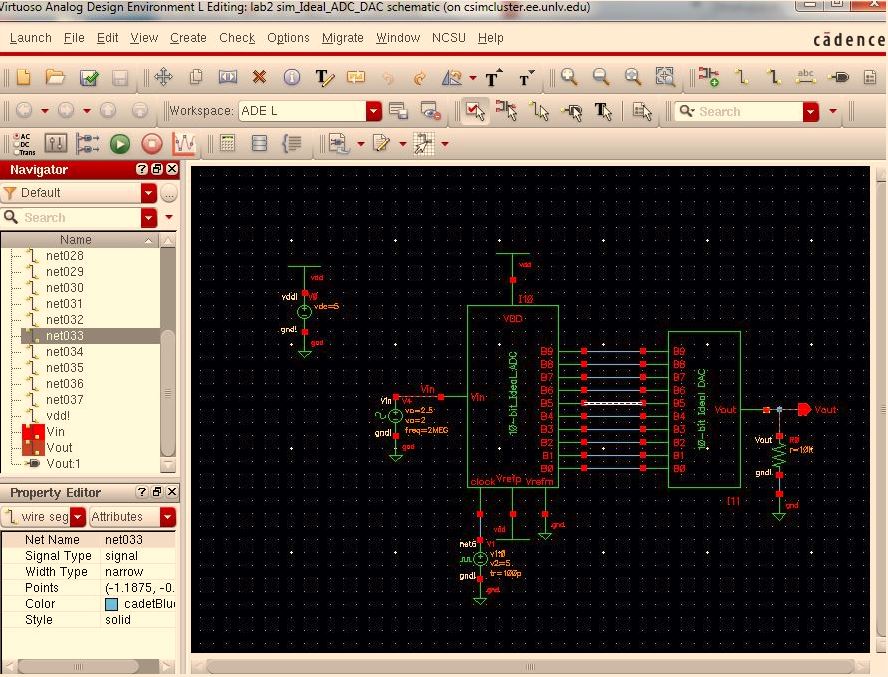
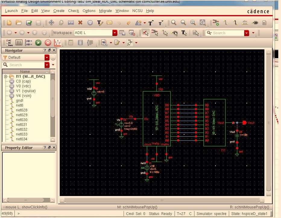
After, selecting lab2, sim_ldeal_ADC_DAC, and Schematic. the following schematic will apear.
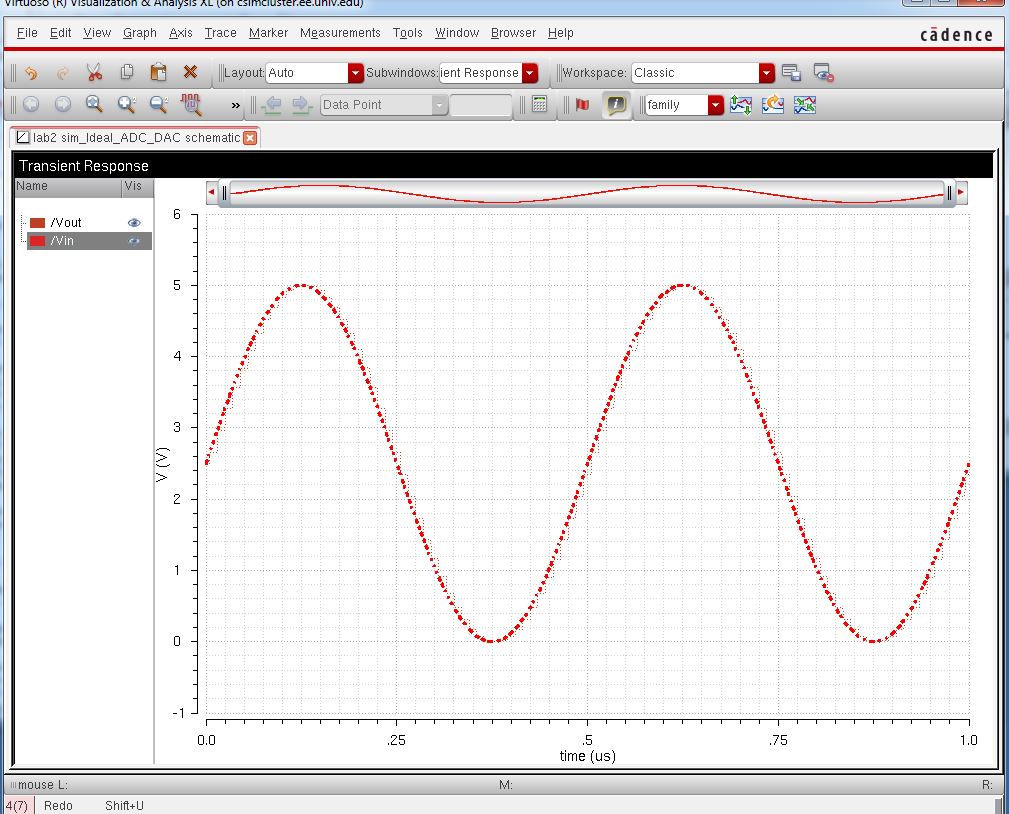
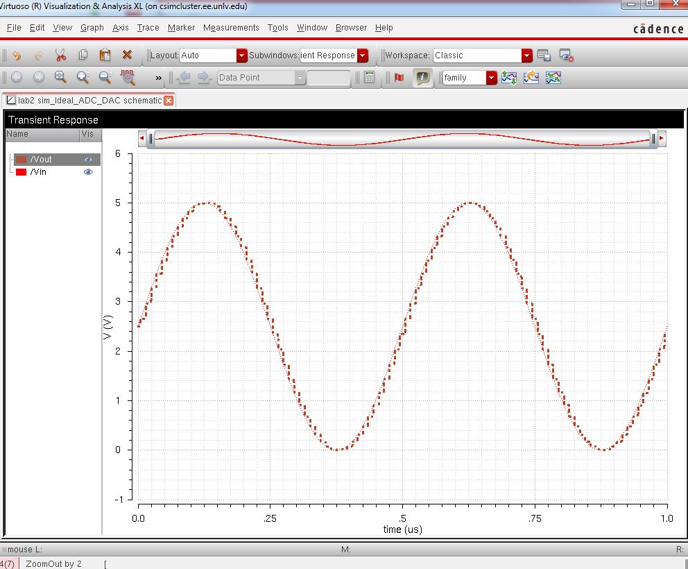
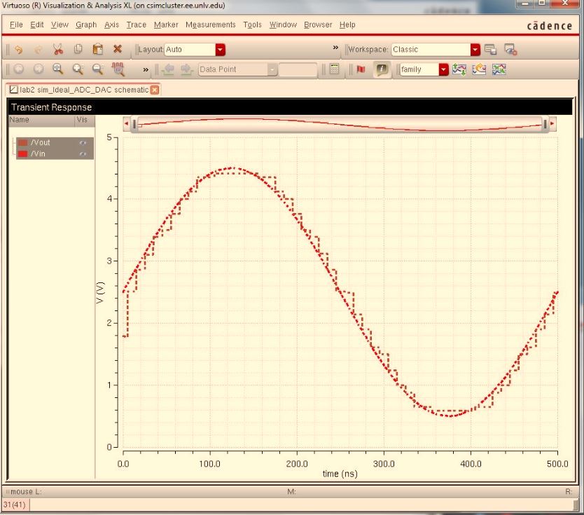
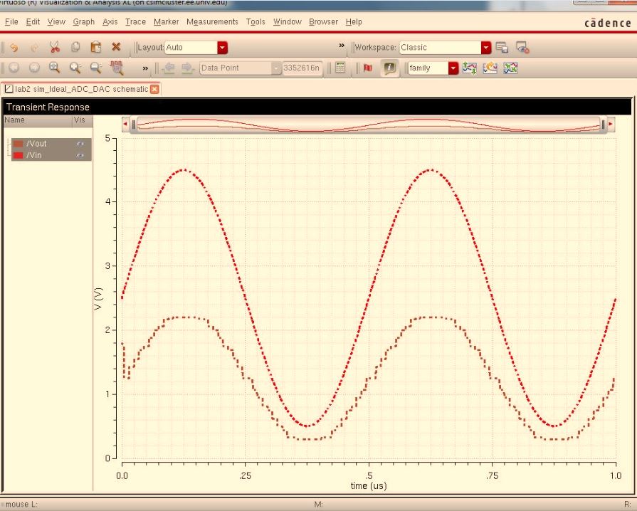
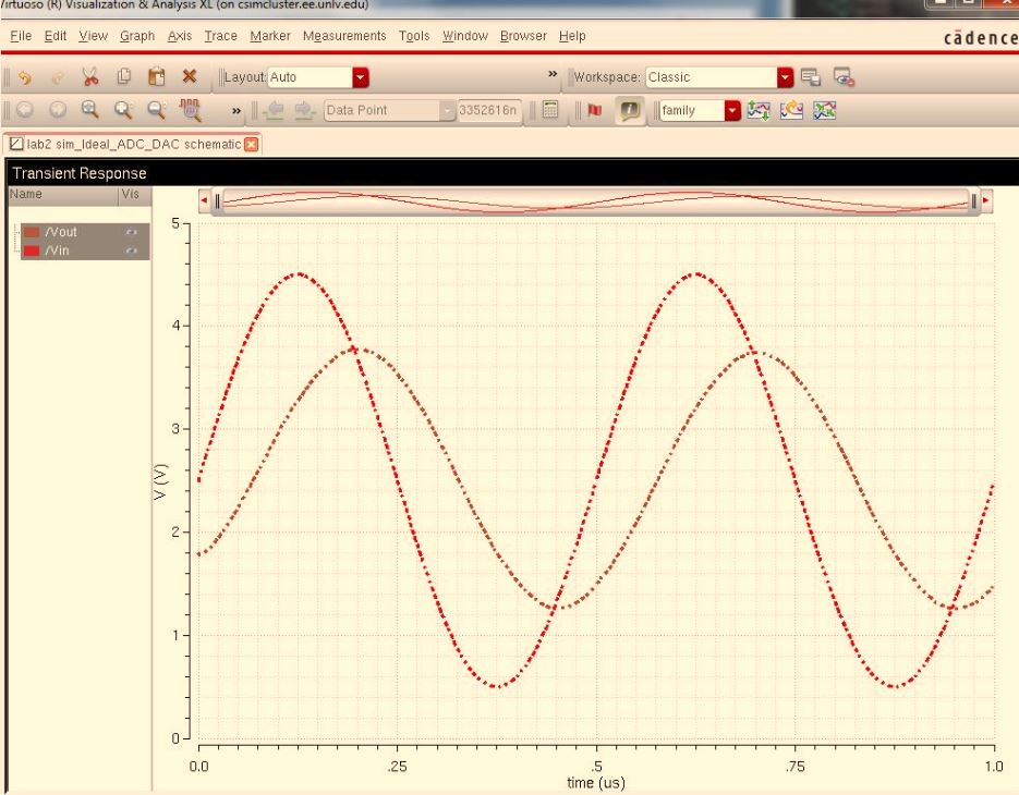
now, it is ready to make run simulation. After simulation the following grap should be apear: if it important we can chage the back groung color.
post lab
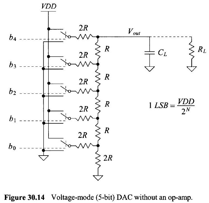
The objective of this lab is to design to a 10-bit DAC using an n-well R of 10k, determine the output resistance of the DAC, and calculating the delay. Our design is based upon the topology seen in Fig. 30.14, which showing blelow.
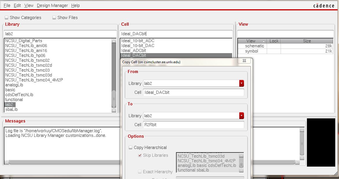
next, create a symbol view for design, which exact the same footprint as the Ideal_10-bit_DAC symbol, so to do that need to make copy of the schematics already provided in Lab2 before drafting design. the following fig showing that copy.
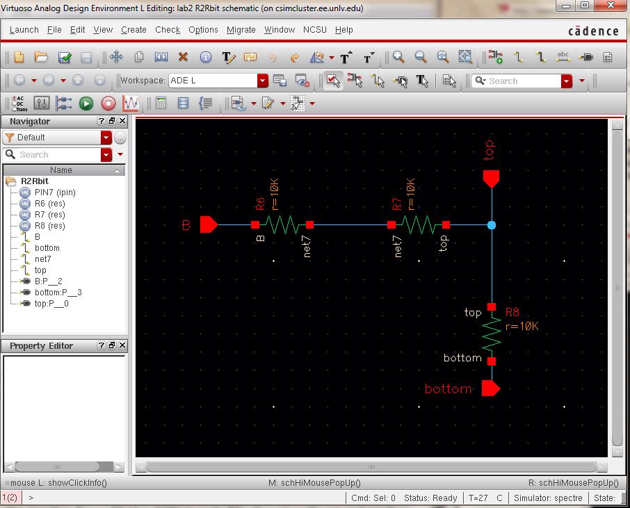
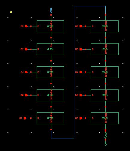
next, creating a voltage divider for the circuit in figure 30.14 in R2Rbit newly file, then place the pin on branch of schematic as seen below.
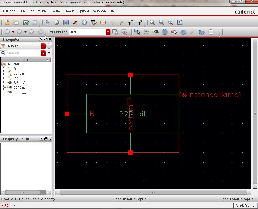
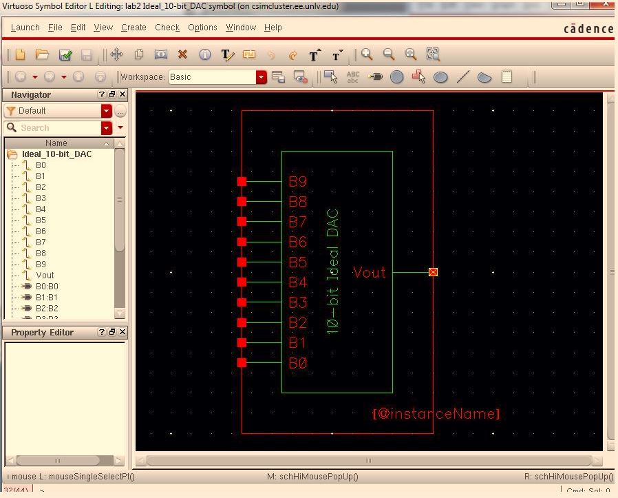
next, we must save check, may have error fix it, does not have error make a symbol, the symbol will apear as follow.
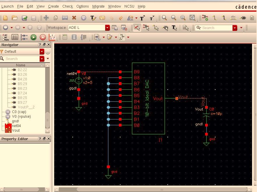
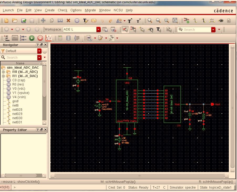
next, make sure save all documents, then copy replace all the 1bit DAC just created.
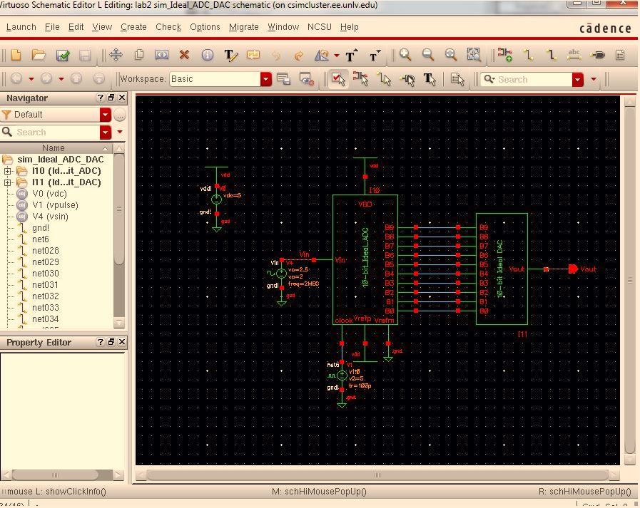
next, we check save, and then replace the ideal DAC with the new one. the new one looks like as follows
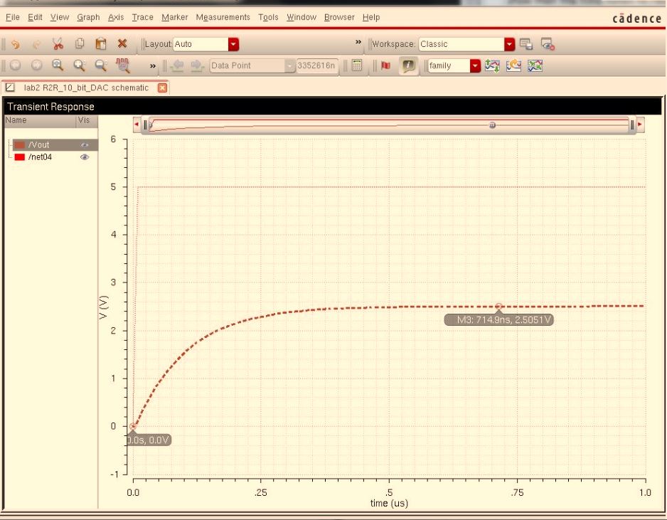
next, save and check then running with the transient simulation for 1us, the result will show below.
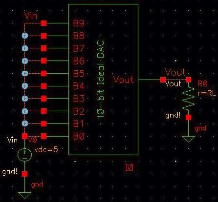
next, to get output resistacnce, using parametric sweep, by setting resistor as RL. the sircuit schematic showing below.
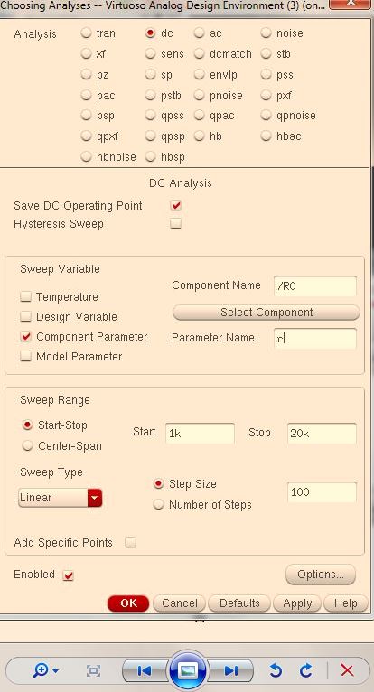
next, the ADL window choosing Analyses, and the resistance assigned tor RL showing below.
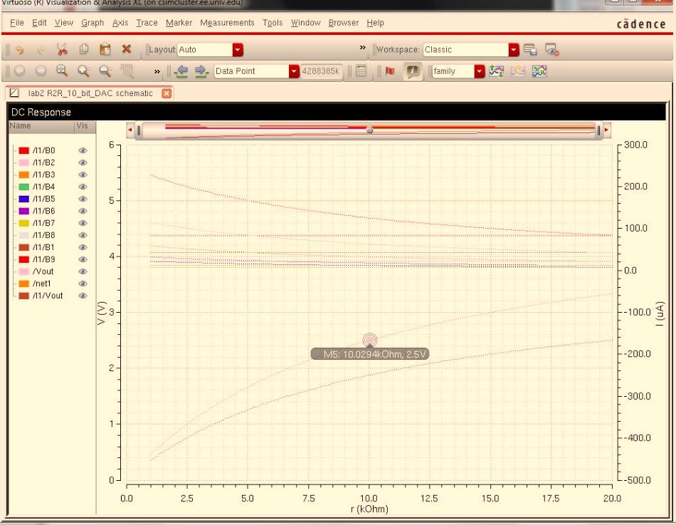
next, Vin=Vout/2, this happen when Rout is 10k. this means the output drop by half of its original output, the DC response showing below.
next, we can expected that the time taken to reach half the value is 0.7RC (0.7*10k*10p=0.7us). this delay happen when the output signal by replaceing the 10k resistor with 10pF, the fig showing below.
next, check and save, then run simulation, the transient response showing below
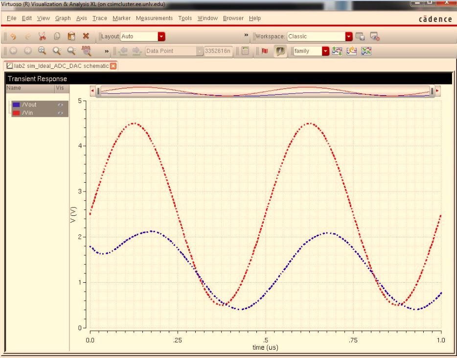
next, by attaching RL the output magnitude should be decreased by half; that showing schemtic ans simulations showing below.
next, by attaching capacitor the signal will delay, and signal have phase shift. also, the capacitor are often used to smooth out singnal, that showing schematic and simulation below.
Indeed, combining capacitor and load resitance will effects decrease the amplitude of the output signal and the phawe delay; showing below simulation and schematic.
to back up the file dragging lab2 from mobxterm to the desktop and e-mail to myself.