Lab 4 - ECE 421L
Authored
by Silvestre Solano,
Email: Solanos3@unlv.nevada.edu
10-6-2014
Generate 4
schematics and simulations
NMOS (6u/600n) device for VGS varying from
0 to 5 V in 1 V steps while VDS varies from 0 to 5 V in 1 mV steps.
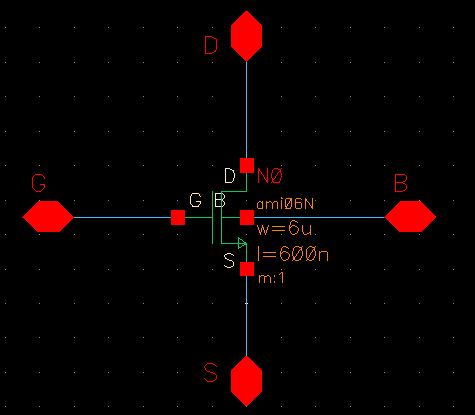
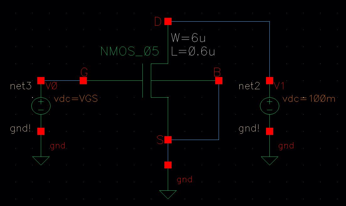
In
order to begin this lab, i must first instatiate a 4 terminal NMOS
device from the analog parts library and then add input/output pins
labeled "B","G","S",and "D". The NMOS device is set to have a width of
6u and a length of 0.6u (600n) and is shown below.
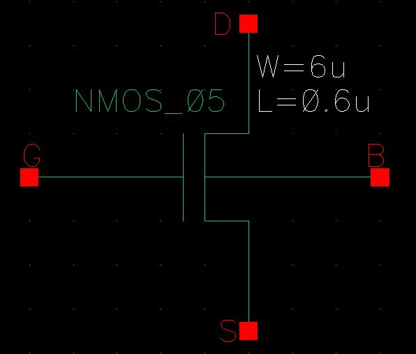
A
symbol is created for the above NMOS device shown below. The symbol
view is named "NMOS 05" because I originally thought I had to make two
NMOS devices and the second one would have been named "NMOS 02", but
this was unnecessary because both NMOS devices have the same
width and length. The "05" refers to sweeping VGS from 0 to 5 and "02"
refers to sweeping VGS from 0 to 2. The same thing happened with the
PMOS device.
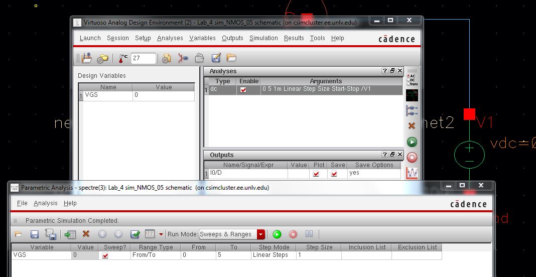
The next step in the lab involves building the schematic shown below in order to perform the simulation.
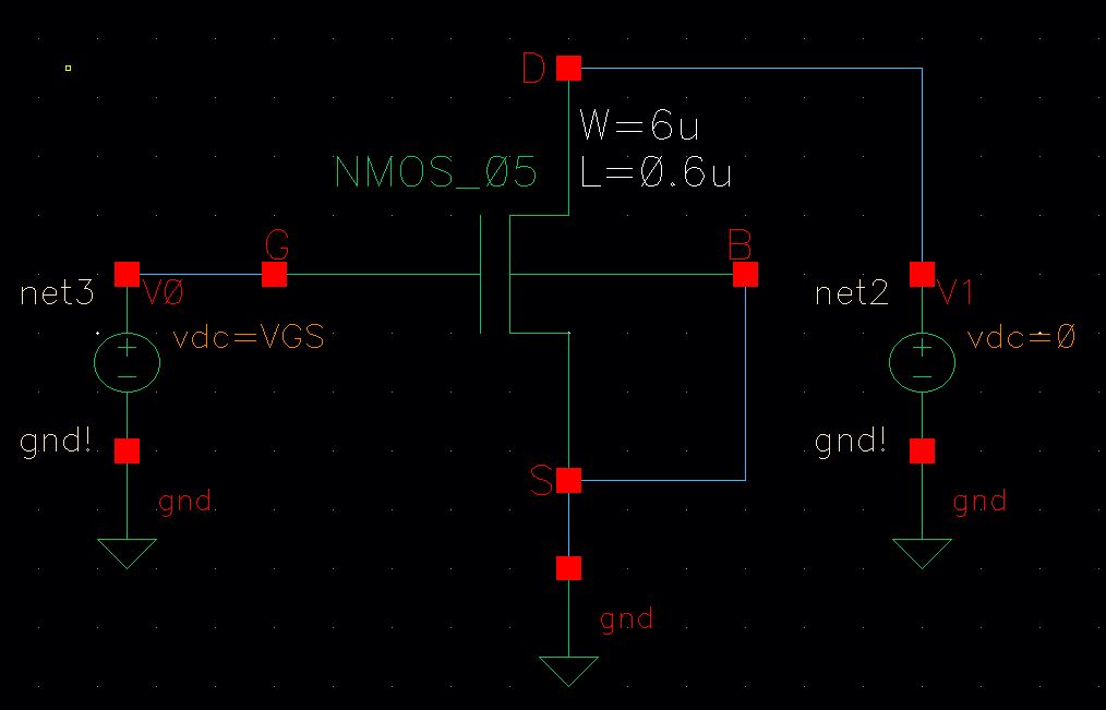
As discused in Tutorial 2, the variable voltage of VGS on V0 must be put in the simulation parameters.
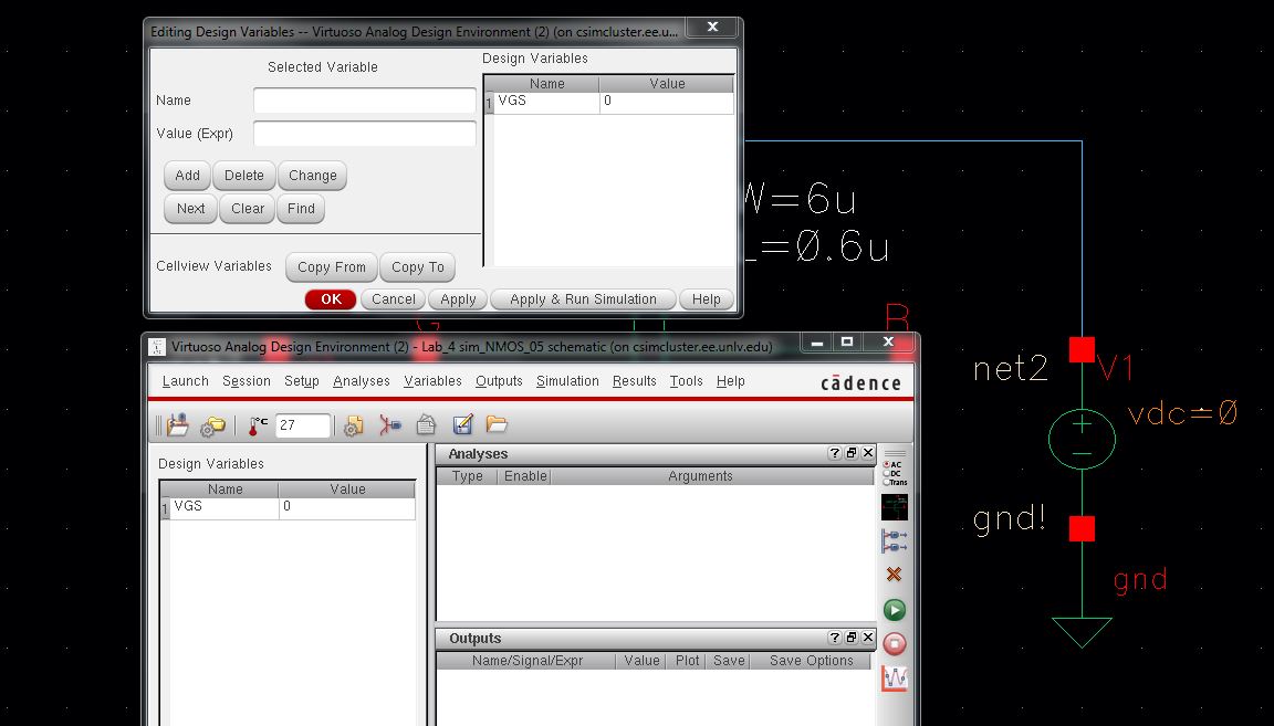
Then,
the voltage source VDS, which in this schematic is labeled as "V1", is
set to sweep from 0 to 5 volts in 1mv steps. VGS is set to sweep from 0
to 5 volts in 1v steps using the parametric analysis tool. The current
of the drain (D) is set to be plotted.
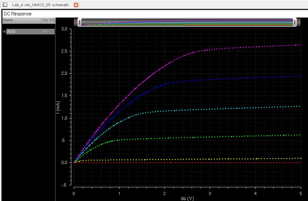
After
the simulation is complete, the following graph appears, which plots
drain current against VDS. Each of the 6 colored plots indicate a
different value of VGS.
NMOS (6u/0.6u) device for VDS = 100 mV
where VGS varies from 0 to 2 V in 1 mV steps.
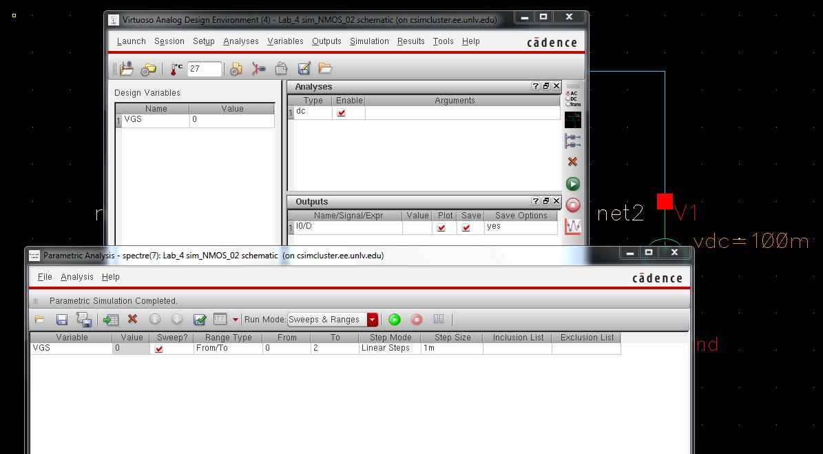
The
second simulation is nearly identical to the previous one except this
one just plots the drain current against VGS, which varies from 0 to 2
Volts at 1mv steps, while VDS stays constant at a value of 100mv. Since
the same NMOS is used, all that has to be done is to create the
schematic to simulate.
The
next step is to set up the simulation parameters. Note that it is not
necessary to use the parametric analysis tool in this part since only
VGS varies and VDS stays constants. Unfortunately for me, I did not
realize this at first and used the parametric analysis tool to sweep
VGS, which took an unusually long time to complete the simulation
because it was going at 1mv steps. If the single sweep is done in the
ADE L, this simulation only takes seconds to complete. So, the
following picture reflects my mistake of using the parametic analysis
tool. I did the same mistake for the PMOS part. However, the results
from the parametric analysis tool are correct, they just take a long
time to complete.
The following is the simulation results. As previously mentioned, they are correct.
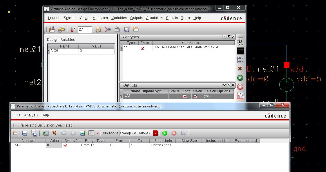
PMOS (12u/0.6u) device
for VSG varying from 0 to 5 V in 1 V steps while VSD varies
from 0 to 5 V in 1 mV steps.
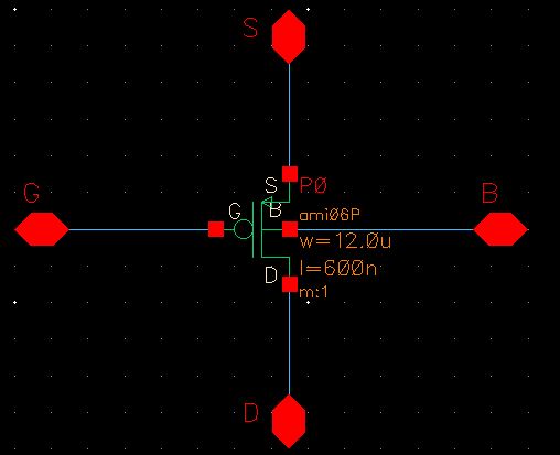
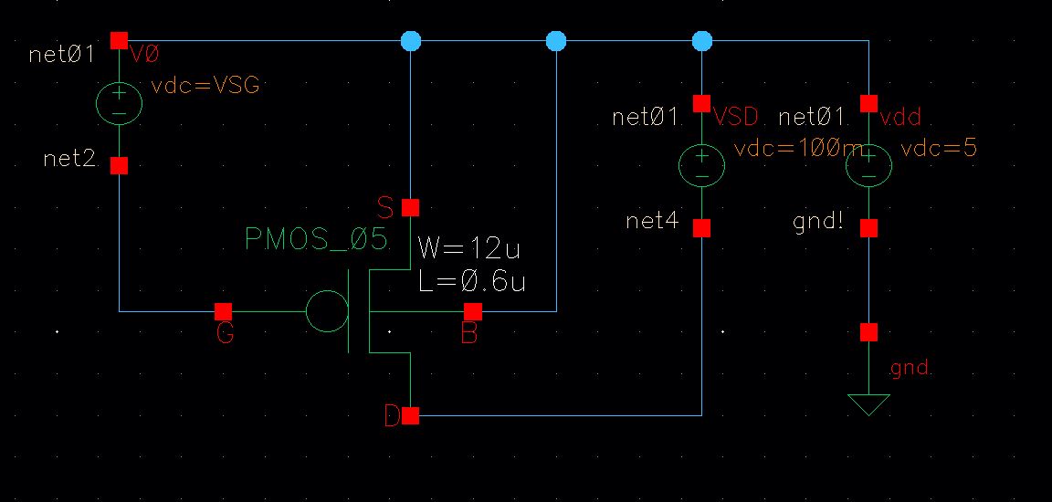
The
PMOS part is virtually identical to the two NMOS schematics and
simulations that were done previously, except it involves the use
of a PMOS instead of an NMOS. And as with the NMOS parts, the PMOS
section begins with the instatiation of a 4 terminal PMOS device from
the analog library and adding 4 input/output pins to labeled "B","S",
"D", and "G".
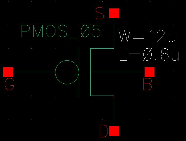
A symbol is created for the PMOS and is shown below.
Then, a schematic is created in order to perform the simulation.
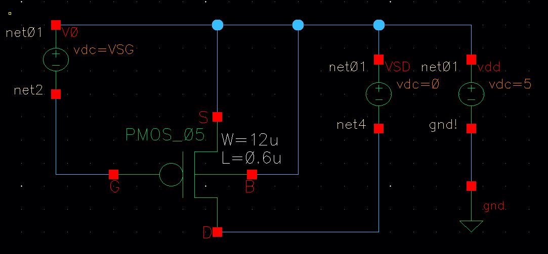
As
before with the NMOS, the simulation is almost the same except the VGS
is now called VSG and VDS is called VSD due to the wacky backwards
nature of the PMOS. VSG is varied from 0 to 5 volts in 1v steps and VSD
is varied from 0 to 5 volts in 1mv steps. VSG is sweeped using the
parametric analysis tool. The simulation parameters are shown below.
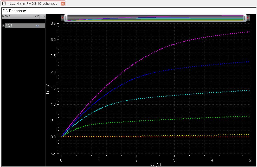
The
simulation results, which plot the drain current againts VDS are shown
below. It is interesting to note that these curves would be upside down
if the current was selected from the node "D" (drain). Instead,they
were selected on the "S" (source) node. This was also done in Tutorial
2.
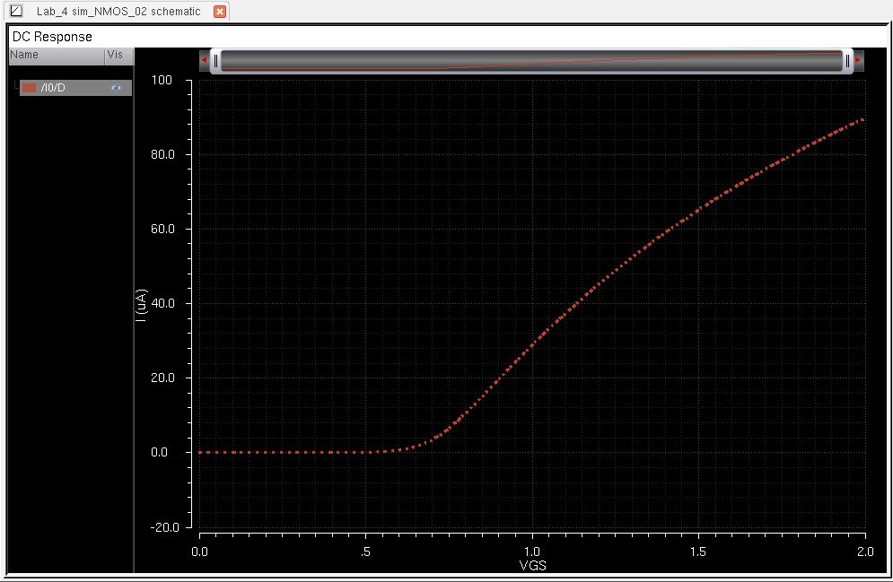
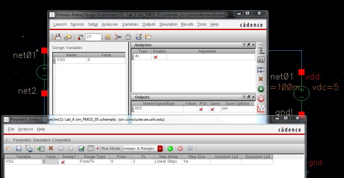
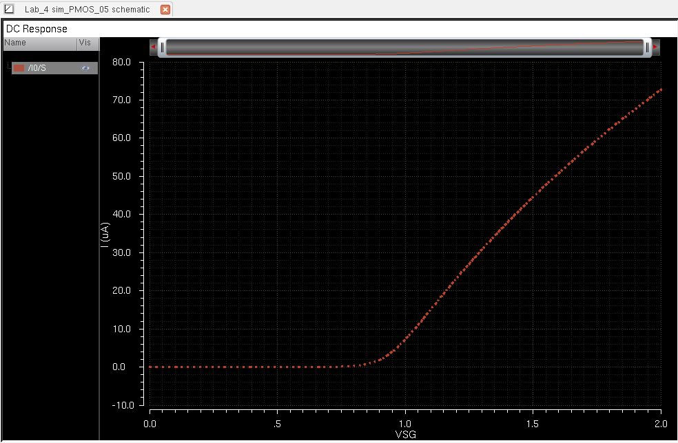
PMOS (12u/0.6u) device for VSD = 100 mV
where VSG varies from 0 to 2 V in 1 mV steps.
The fourth simulation is nearly identical to the previous one except this
one just plots the drain current against VSG, which varies from 0 to 2
Volts at 1mv steps, while VSD stays constant at a value of 100mv. The following circuit shows the setup for the simulation.
The simulation parameters are shown below. VSG is
varied from 0 to 2 volts in 1mv steps and VSD is constant at 100mv. The simulation parameters are shown below. Contrary to the following picture, due not use the parametric analysis tool.
The
simulation, which plots drain current against VSG, is shown below.
There is only one plot on this graph because VSD is constant.
Lay out a
6u/0.6u NMOS device and connect all 4 MOSFET terminals to probe pads
Show your layout passes DRCs
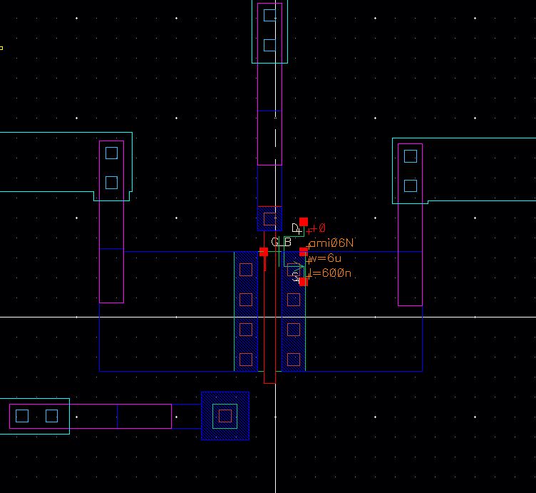
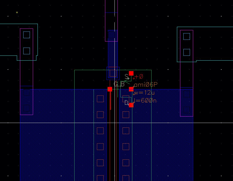
To
begin the layout of the NMOS, I will instatiate a basic one from the
ami 06 library. Then I changed its length and width to 6u/0.6u.
Afterwards, metal 1 Pins labeled "B", "G" ,"S", and "D" will be added to
the corresponding parts on the layout. The probe pads, which were
created by professor Baker, are made of metal 3 and are attached to
each pin by a series of metal 3 connected to metal 2 connected to metal
1. Each metal-to-metal connection is done with the corresponding vias. A
ptap was created for the "B" (body) connection and the poly layer was
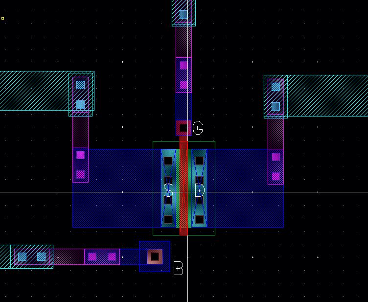
streched in order to use a poly to metal 1 via. A zoomed in view of the completed layout is shown below. The probe pads are not shown in the zoomed in view.
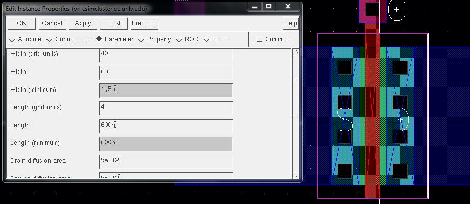
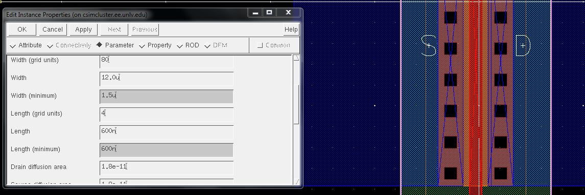
The setting of the width and length is shown below.
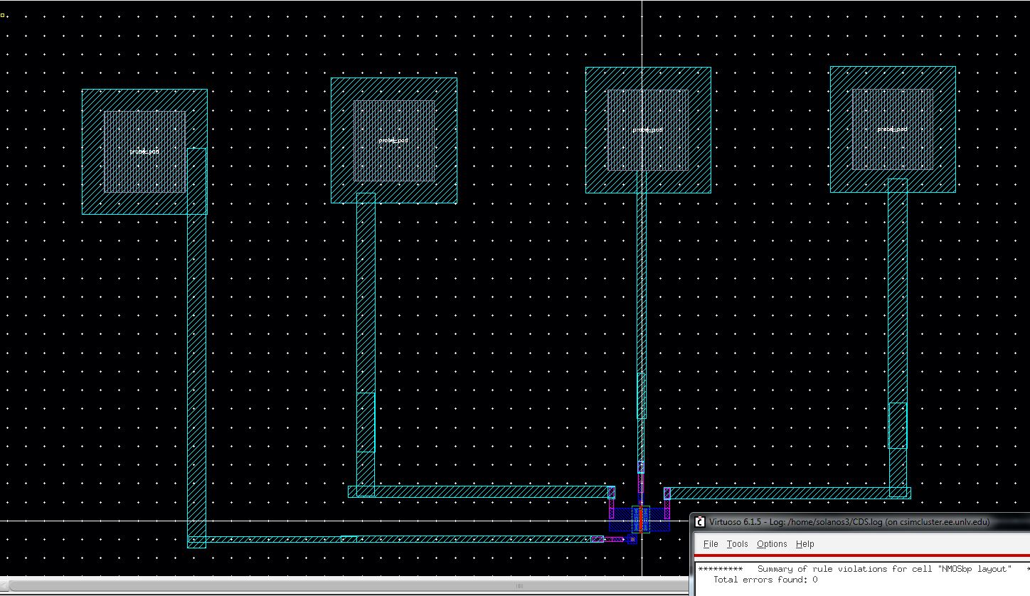
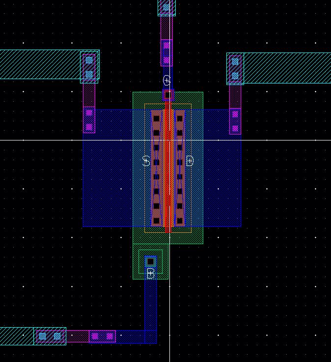
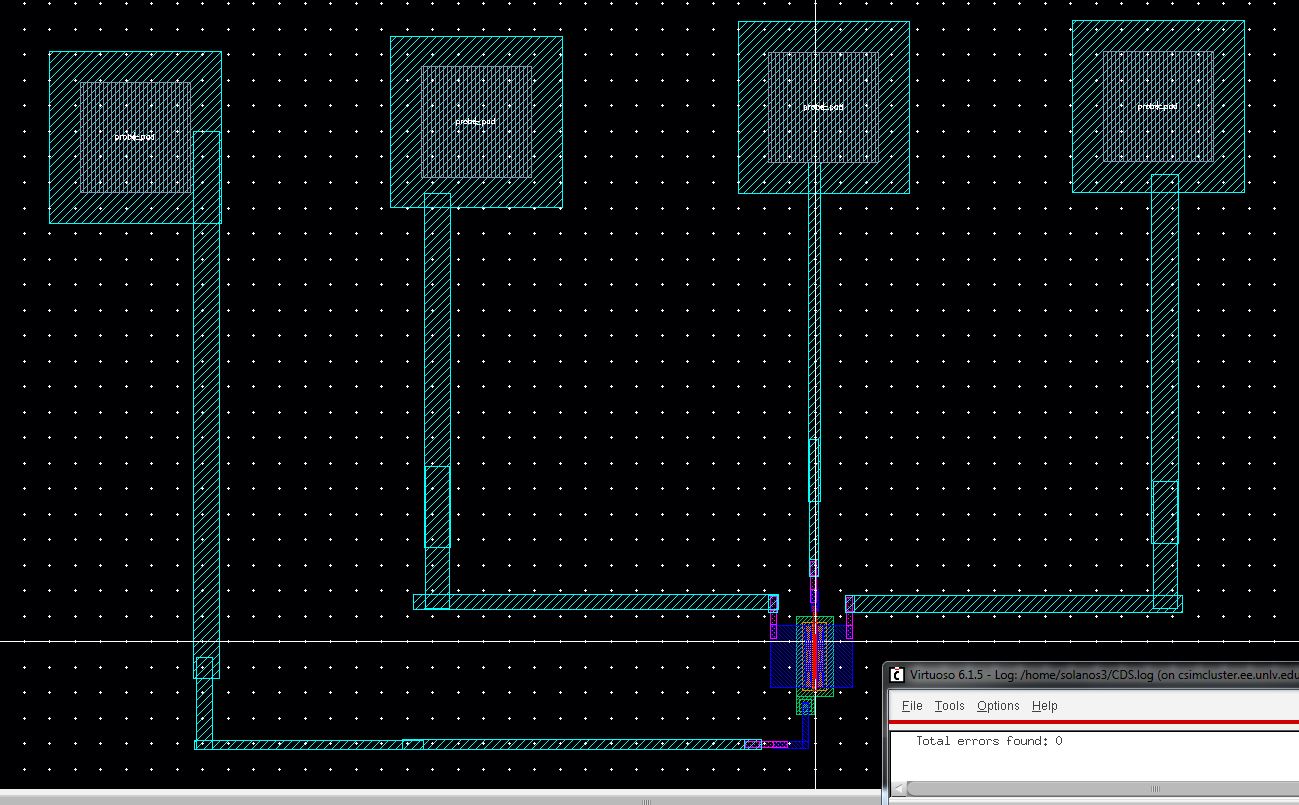
After
connecting the probe pads to a far enough distance, the DRC command was
used and it completed succesfully. The entire layout with the probe
pads attached and the command interpreter window, showing that the DRC
passed with no errors, is shown below. The command interpreter window
is on the bottom right corner.
Make a corresponding schematic so you
can LVS your layout.
The layout was extracted and the resulting extraction, which will be used for the LVS, is shown below.
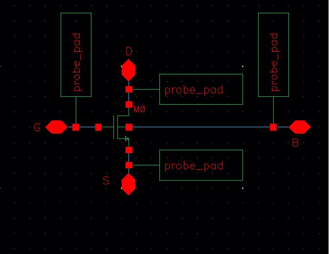
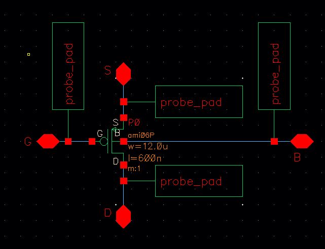
The
schematic was creted simply by instatiating a 4 terminal NMOS from the
analog parts library, changin its width to 6u and length to 0.6u,
and attaching the 4 pins labeled "B", "G", "S", and "D". The probe pads
are identical to the ones professor Baker created and placed in the Lab
4 instructions. I just basically copied their schematic and symbol and
attached them to my schematic as shown below.
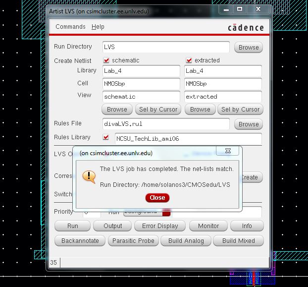
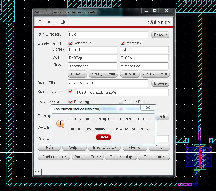
LVS
is used to compare the schematic and the extracted layout shown
previously and it completed succesfully with matching net-lists. The
proof is shown below.
Lay out a
12u/0.6u PMOS device and connect all 4 MOSFET terminals to probe
pads.
Show your layout passes DRCs.
The
layout of the PMOS follows the identical procedure as the layou of the
NMOS. I will instatiate a basic PMOS from the ami 06 library. Then
I changed its length to 12u and width 0.6u. Afterwards, metal 1
Pins
labeled "B", "G" ,"S", and "D" will be added again to
the corresponding parts on the layout. The probe pads are made of metal 3 and are attached to
each pin by a series of metal 3 connected to metal 2 connected to metal
1. An ntap was created for the "B" (body) connection and the poly layer was
streched in order to use a poly to metal 1 via. A zoomed in view of the completed layout is shown below.
The setting of the width and length are shown below.
Using
the DRC command, the DRC check found no errors. The picture below shows
the entire layout, with the probe pads attached, and the command
interpreter window showing that the DRC check found no errors.
Make a corresponding schematic so
you can LVS your layout.
The PMOS layout was extracted and its extraction is shown as follows.
The
corresponding schematic was done just as the NMOS. The 4 terminal PMOS
was instatiated from analog parts library and the pins labeled "B",
"G", "S", and "D" are added. Its lenght is changed to 12u and width is
set to 0.6u. The probe pads are attached and the entire schematic is as
follows.
The
schematic and extracted layout are compared using the LVS and the
comparison was completed successfully with matching net-lists. The
proof is shown below.
This basically concludes Lab 4.
As always, all my work is backed up to my flash drive and laptop.
My completed Lab 4 folder can be found in this zip file.
Return to the main Lab directory.