In this lab we will be creating the layout for the 1-bit DAC we used in Lab 2. In that lab, we assumed that we would be using the NCSU 10k resistors. After this lab is finished, we will be replacing the NCSU 10k resistors with ones that we create in the n-well. By following the steps in Tutorial 1 we will build the 10k resistor layout and then will implement that resistor in the layout for our 1-bit DAC. To get started we are going to copy over the entire library from Lab 2 into a new library called Lab 3 so we can compare our results later.
First thing we need to do is create the 10k n-well resistor. We make a new layout file named R_n_well_10k and open that to create our 10k resistor. This will allow us to make changes to this layout and it will propagate throughout whatever other layouts we place it in.

Once the layout opens select the n-well layer and create a rectangle with and dimsnsions you want because we wil be changing those next.

Also, we can see that the minimum width is 12 Lambda and the minimum space needs to be 18 Lambda.
width = 12*300nm = 3.6um minimum
space = 18*300nm = 5.4um minimum

Next, we need to create a width and length that will give us the resistance we want while also being evenly divisible by 1.5um. From the MOSIS specs we see that the sheet resistance of the n-well is about 800 squares. If we choose 4.5 as a width and 56.1 as a length this will satisfy both conditions. Once we have the rectangle dimensions fixed we can run a DRC to make sure that we aren't violating any of the rules.
R = Rsquare * (l/w) = 800 * (56.1/4.5) = 9973 ~= 10k
56.1/.15 = 374
4.5/.15 = 30


Once we pass the DRC we can add the n-tap on either end. Press I, go to the NCSU_Techlib_ami06 library and select the ntap. Once selected change the number rows of contacts to 2 and place on on either side of the n-well rectangle.

DRC then we are going to add the pins to the ends of the resistor so we can connect to it. select the metal 1 layer, and select create --> pin from the menu. Draw a rectangle covering the metal 1 layer on the left and call it L. Then do the same to the one on the right and label it R.

DRC again to ensure no mistakes and then we are going to add the final layer. Select res_id and then draw a rectangle that fully covers the first rectangle we drew in the n-well. This will tell Cadence that this part is supposed to be used as a resistor.

After DRC a final time we can extract the layout. Select Verify-->Extract and extract the layout. This extracted layout will give us the resistance which should be about 10k.

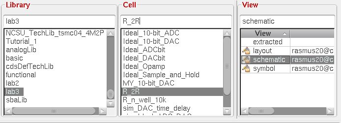
Following the tutorial we are next going to create a resistive divider. We need to create a new layout named R_2R. Once that has opened we will press I and insert three instances of the 10k n-well resistor we just created while making sure they are spaced far enough apart to satisfy the design rules.


Next we are going to select the metal 1 layer and draw some rectangles to connect the resistors together. We will make a rectangle coming out the top left of the top resistor, one connecting the right sides of the top and middle resistor, one connecting the left sides of the middle and bottom resistor, and finally one coming out of the bottom right of the bottom resistor.

Over these rectangle we are going to create some pins and label them. It is very important to make sure that we make the pins exactly the same as they designated in the R_2R schematic. The top left pin will be labeled as in and tagged as an input. The pin connecting the middle resistor to the bottom one will be labeled top and will be tagged input/output. The pin on the bottom right of the bottom resistor will be labeled bottom and weill also be tagged input/output.

Now we need to DRC again and make sure there are no errors.

Now we need to save and do an LVS check to make sure the layout matches the schematic we created in Lab 2. Select Verify--> LVS and make sure it passes.


Here is a link to the files used in this lab.
Return to 421L Homepage