Lab 7 - EE 421L
Using Buses and Arrays in the Design of Word Inverters, Muxes, and High-Speed Adders
Pre-Lab
Review Tutorial 5 which can be found here.
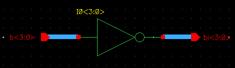
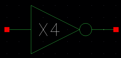
Design & Simulation of a 4-bit Word Inverter
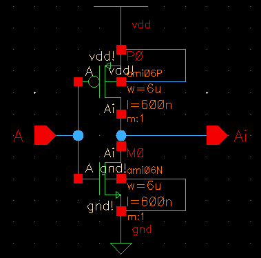
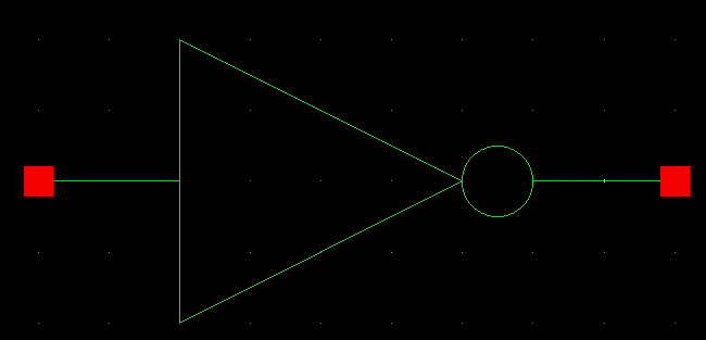
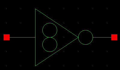
1 Bit Inverter
| Verification |
||
| Schematic |
|
|
| Symbol |
|
|
| Verification |
||
| Schematic |
 |
 |
| Symbol |
 |
 |
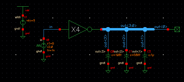
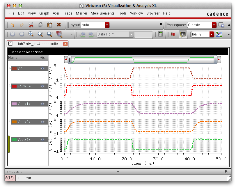
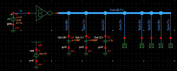
Notice the increase of signal delay from out<0> to out<3> this is due to increasing output capacitance.
Imagine the capacitor as a bucket and charge as water, the bigger the bucket the longer it takes to fill it with water.
The greater the capacitance the greater the delay.
Design and Simulation of an 8 bit NAND Gate
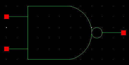
1 Bit Input/Output NAND Gate
| Verification |
||
| Schematic |
 |
 |
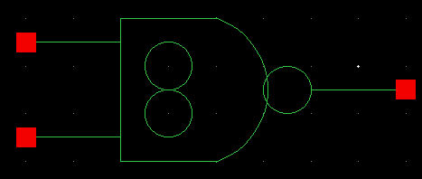
| Symbol |
 |
 |
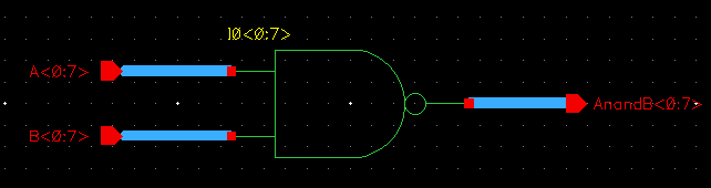
8 Bit Input/Outut NAND Gate
| Verification |
||
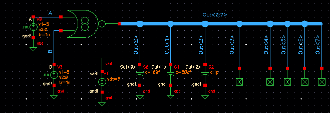
| Schematic |
 |
 |
| Symbol |
 |
 |
8 Bit NAND Simulation
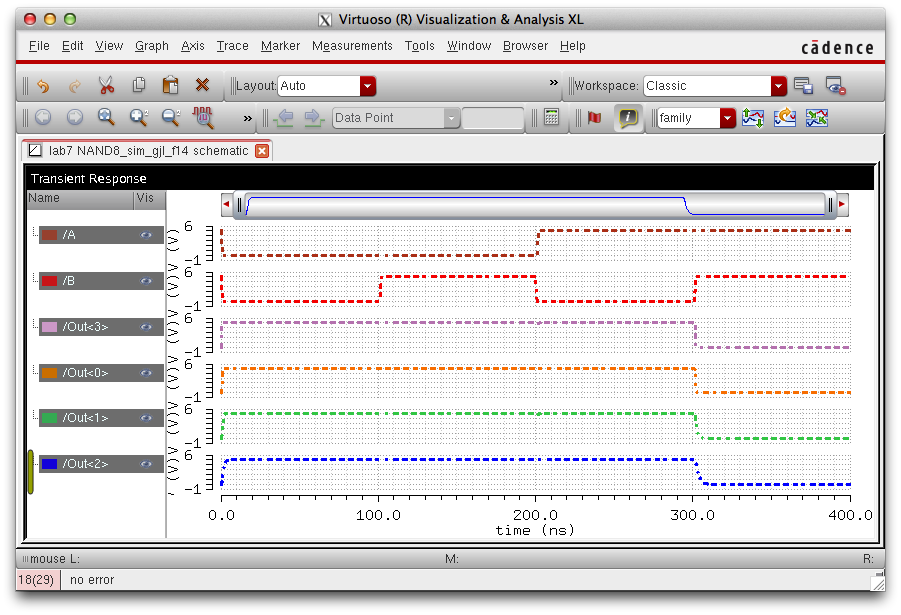
Notice the increase of signal delay from out<0> to out<3> this is due to increasing output capacitance.
Imagine the capacitor as a bucket and charge as water, the bigger the bucket the longer it takes to fill it with water.
The greater the capacitance the greater the delay.
Design and Simulation of an 8-bit NOR Gate
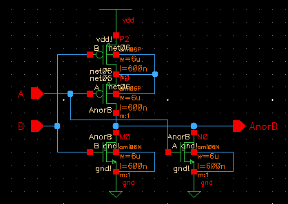
1 Bit Input/Output NOR Gate
| Verification |
||
| Schematic |
 |
 |
| Symbol |
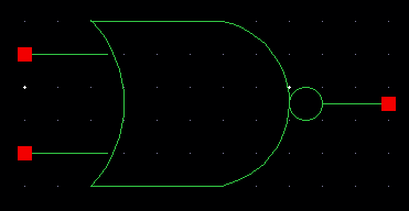 |
 |
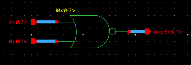
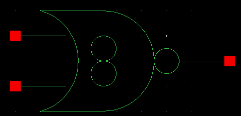
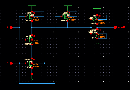
8 Bit Input/Output NOR Gate
| Verification |
||
| Schematic |
 |
 |
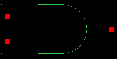
| Symbol |
 |
 |
8 Bit NOR Simulation
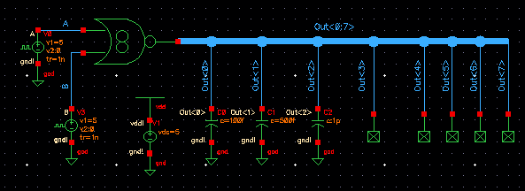
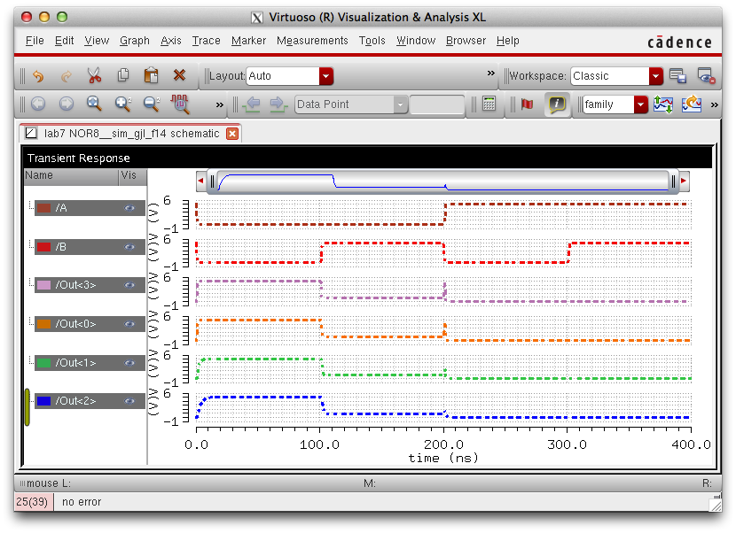
Notice the increase of signal delay from out<0> to out<3> this is due to increasing output capacitance.
Imagine the capacitor as a bucket and charge as water, the bigger the bucket the longer it takes to fill it with water.
The greater the capacitance the greater the delay.
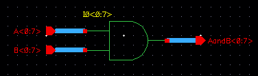
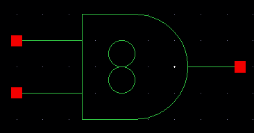
Design & Simulation of an 8-bit AND Gate
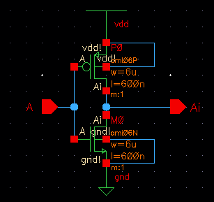
1 Bit Input/Output AND Gate
| Verification |
||
| Schematic |
 |
 |
| Symbol |
 |
 |
8 Bit Input/Output AND Gate
| Verification |
||
| Schematic |
 |
 |
| Symbol |
 |
 |
8 Bit AND Simulation
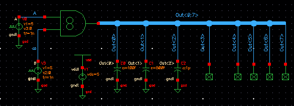
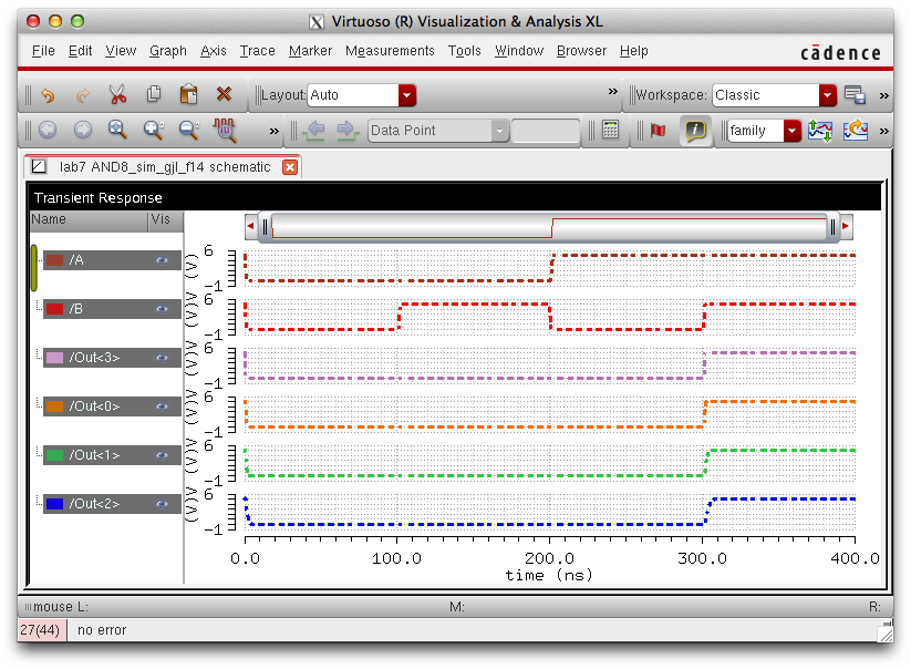
Notice the increase of signal delay from out<0> to out<3> this is due to increasing output capacitance.
Imagine the capacitor as a bucket and charge as water, the bigger the bucket the longer it takes to fill it with water.
The greater the capacitance the greater the delay.
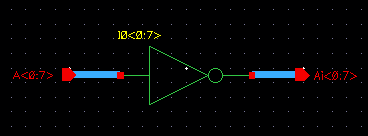
Design & Simulation of an 8 bit Inverter
1 Bit Input/Output Inverter
| Verification |
||
| Schematic |
 |
 |
| Symbol |
 |
 |
8 Bit Input/Output Inverter
| Verification |
||
| Schematic |
 |
 |
| Symbol |
 |
 |
8 Bit Inverter Simulation
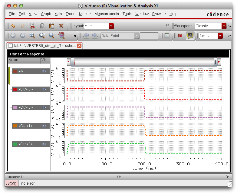
Notice the increase of signal delay from out<0> to out<3> this is due to increasing output capacitance.
Imagine the capacitor as a bucket and charge as water, the bigger the bucket the longer it takes to fill it with water.
The greater the capacitance the greater the delay.
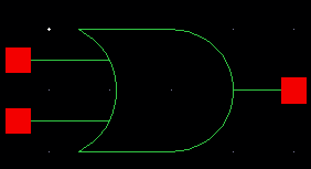
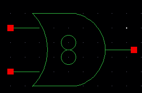
8 Bit OR Gate Design & Simulation
1 Bit Input/Output OR Gate
| Verification |
||
| Schematic |
 |
 |
| Symbol |
 |
 |
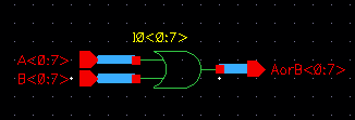
8 Bit Input/Output OR Gate
| Verification |
||
| Schematic |
 |
 |
| Symbol |
 |
 |
8 Bit OR Gate Simulation
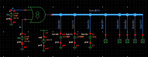
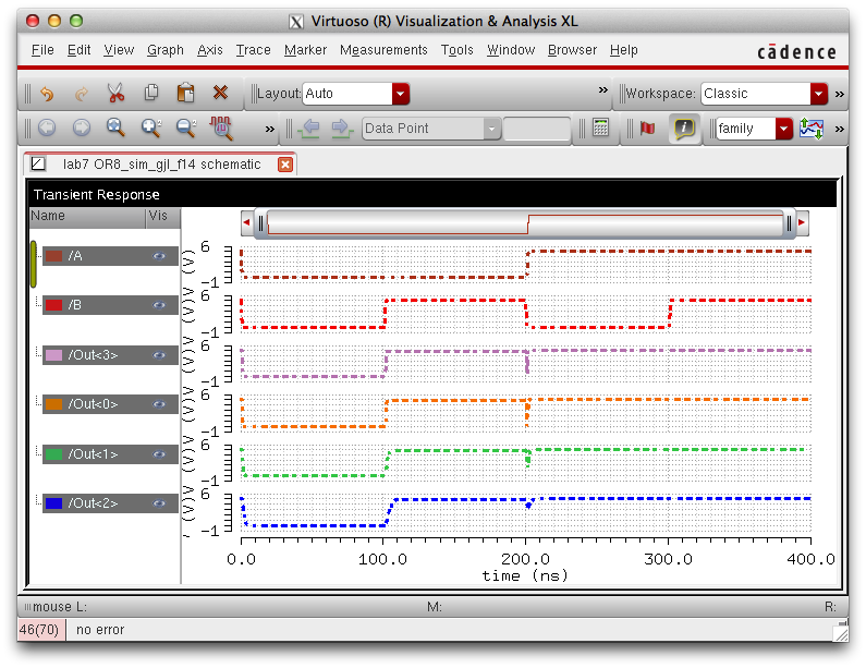
Notice the increase of signal delay from out<0> to out<3> this is due to increasing output capacitance.
Imagine the capacitor as a bucket and charge as water, the bigger the bucket the longer it takes to fill it with water.
The greater the capacitance the greater the delay.
2 to 1 MUX/DEMUX Operation
Mux Operation/Simulation
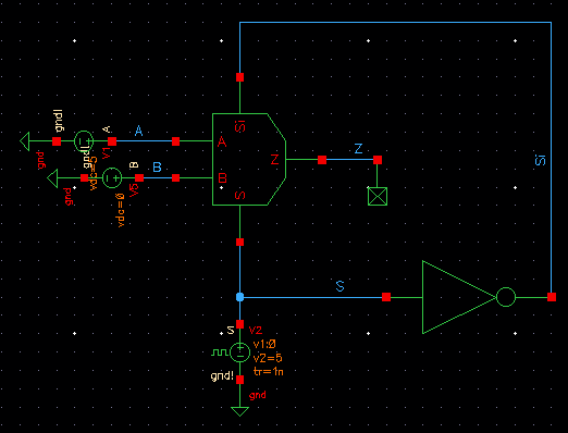
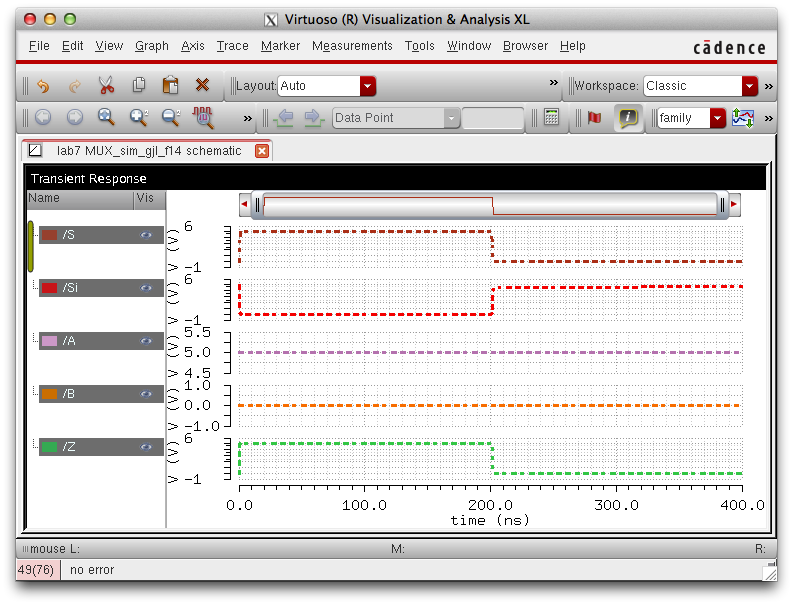
The purpose of a MUX is to output one signal from multiple input signals.
Observe the Plot above, Signal A= 5V & Signal B =0V
Notice when S (Select) = 1 that Z (Output)= 5V
Notice when S(Select) = 0 that Z (Output) = 0V
DEMUX Operation/Simulation
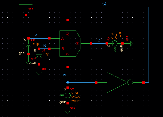
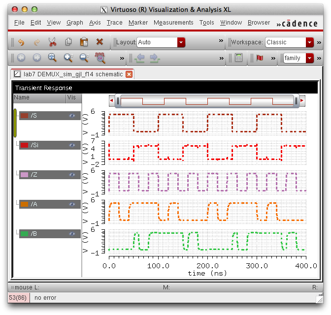
The purpose of a DEMUX is to choose an ouput path based on multiple outputs given one incoming signal.
Observe the Plot above:
Notice when S (Select) = 1 that A(Output)= Z (Input)
Notice when S (Select) = 0 that B(Output)= Z (Input)
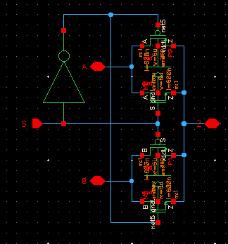
Design & Simulation of an 8-Bit MUX/DEMUX
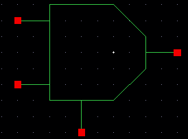
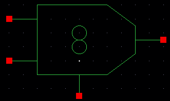
1 bit Input/Output MUX/DEMUX
| Verification |
||
| Schematic |
 |
 |
| Symbol |
 |
 |
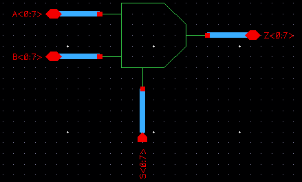
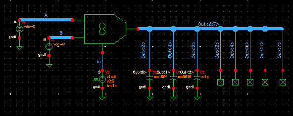
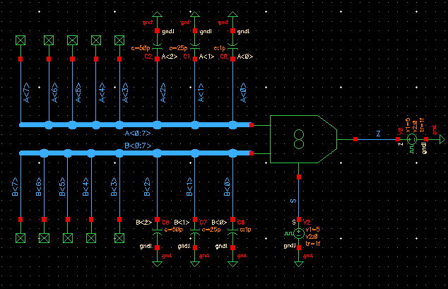
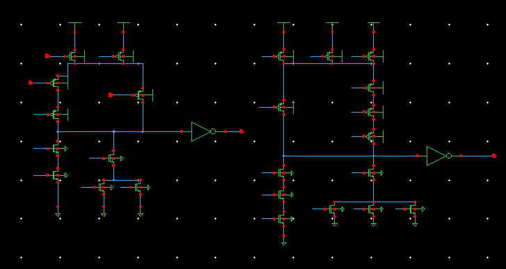
8 Input/Output MUX/DEMUX
| Verification |
||
| Schematic |
 |
 |
| Symbol |
 |
 |
8 Bit Input/Output MUX Simulation
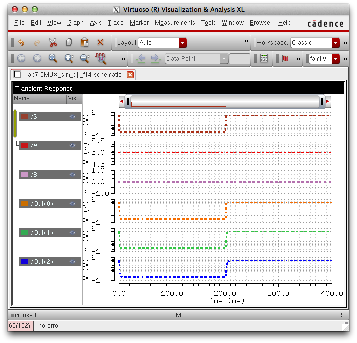
Notice the increase of signal delay from out<0> to out<3> this is due to increasing output capacitance.
Imagine the capacitor as a bucket and charge as water, the bigger the bucket the longer it takes to fill it with water.
The greater the capacitance the greater the delay.
8 Bit Input/Output DEMUX Simulation
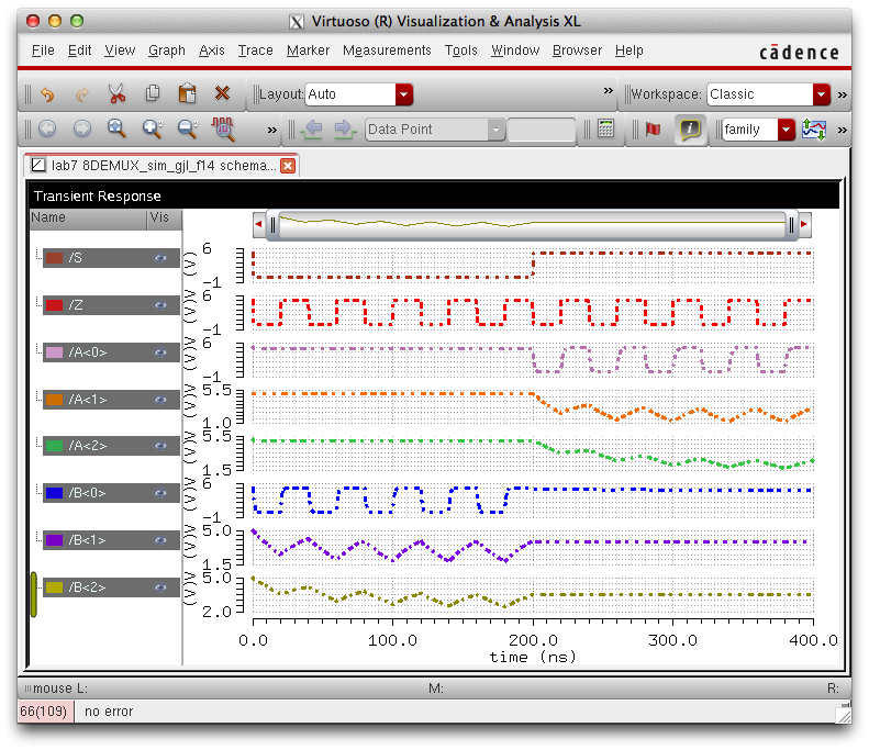
Notice
the increase of signal delay/distortion from A<0> to A<2>
and from B<0> to B<3>, this is due to increasing output
capacitance.
Imagine the capacitor as a bucket and charge as water, the bigger the bucket the longer it takes to fill it with water.
The greater the capacitance the greater the delay.
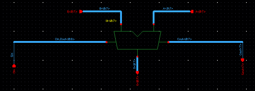
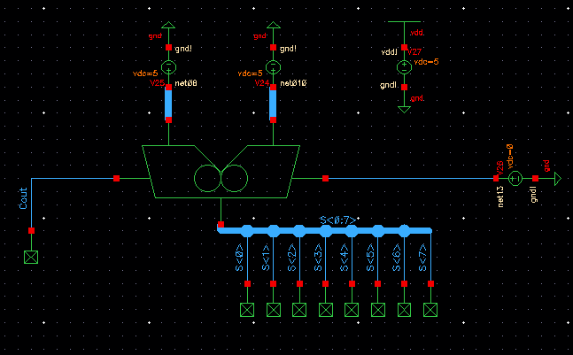
Design & Simulation of a 8-Bit Full Adder
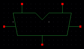
1 Bit Input/Output Full Adder
| Verification |
||
| Schematic |
 |
 |
| Symbol |
 |
 |
| Verification |
||
| Schematic |
 |
 |
| Symbol |
 |
 |
8 Bit Full Adder Simulation
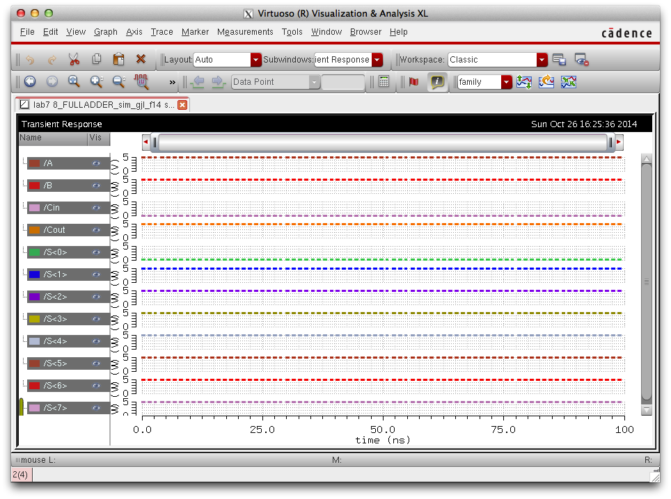
Observe from the plot above that we are adding A= 11111111 and B=11111111 with a Cin of=0.
Output= 11111110 with a Cout of= 1 as expected our 8-bit Full Adder is working correctly.
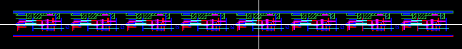
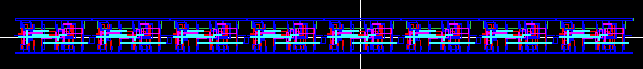
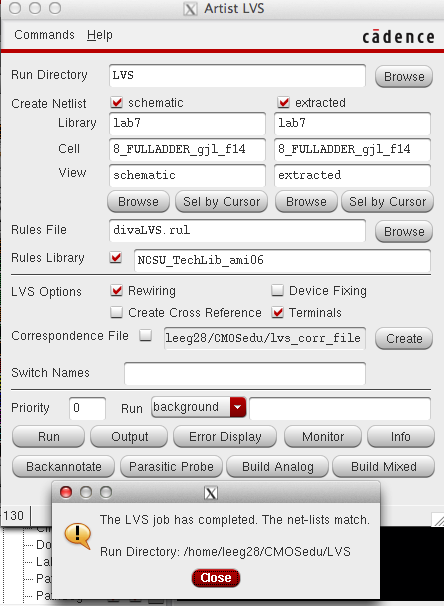
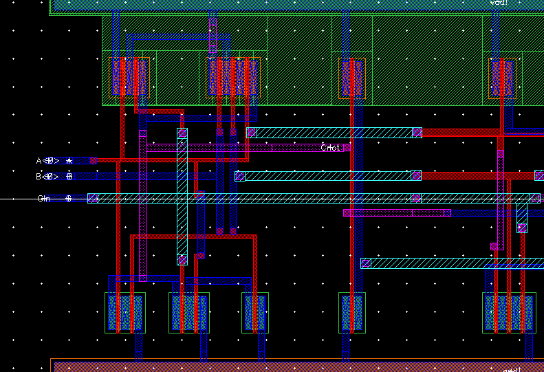
Layout of an 8-bit Full Adder
| Verifcation |
||
| Schematic |
|
|
| Symbol |
|
|
| Layout |
 |
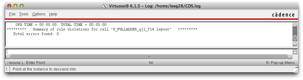 |
| Extracted |
 |
 |
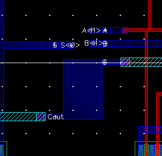
View of One Adder Cell
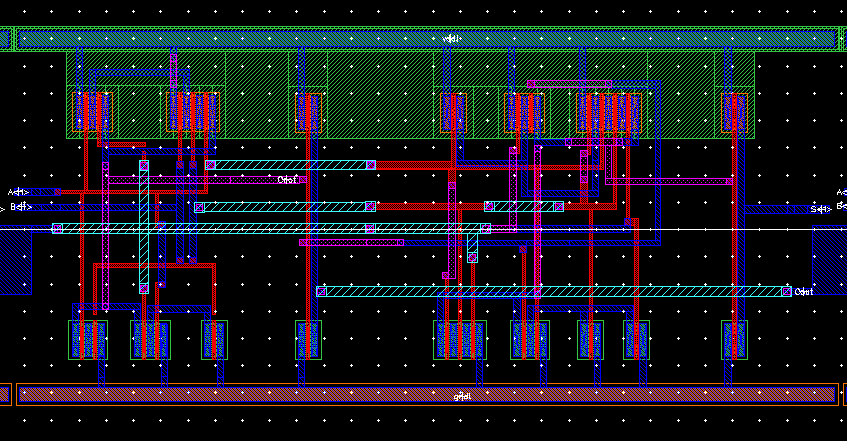
Left View of 8-Bit Full Adder
Right View of 8-Bit Full Adder
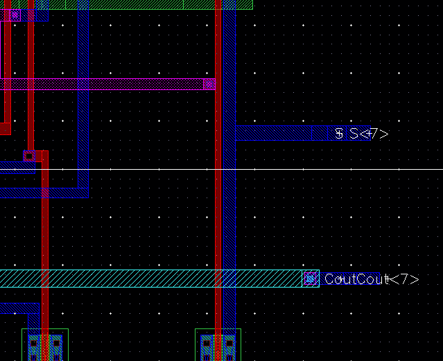
View of Carry Out to Carry In Signal Propagation between each Adder Cell
This concludes the lab, design files can be found here.
Back-Up of Lab 7 is shown below: