ALU Design - ECE 421L Project
Authored
by, Vincent Ibanez
Email: ibanez.troy.e@gmail.com
Today's
date 11/9/2014
In
this project we designed and simulated an 8-bit ALU that can
perform: A AND B, A OR B, A + B (addition), and A - B (subtraction).
Details of the operation is listed below:
| F0 | F1 | Operation |
| 0 | 0 | A AND B |
| 0 | 1 | A OR B |
| 1 | 0 | A + B |
| 1 | 1 | A - B |
The top level ALU
symbol used for simulations have the following inputs (all bus
connections): A (8-bits), B (8-bits), F (2 bits), and Z (8-bits).
The components used in the design were derived from the Components Designed in Lab7.
The components used from lab 7 are listee below:
- 8-bit AND gate
- 8-bit OR gate
- 8-bit 2to1 Multiplexer
- 8-bit Full Adder
- 8-bit Inverter
The schemtic was designed using Cadence Virtuoso Schematic Editor and shown below:
In
this design, the 2to1 MUX before the output z determines whether the
operation will be a logic (AND, OR) or arithmetic(+, -) operation. It
is controlled by F0.
The
8-bit logic gates are hooked up to another MUX which simply selects
wheter to pass AND or OR gate signals. This is controller by F1.
The
arithmetic operations are simplified by using a Full Adder for both
addition and subtraction operations. Note that a subtraction operation
A - B is equivalent to A + (-B). The negative of a number obtained by
taking its one's complement. This is implemented in the design by
connecting B input into an 8-bit inverter and adding a 1 to the carry
in whenever there is a subtraction operation. The MUX that B is
connected to simply selects whether to add a +B or a -B.
Simulations
In order to check the simulations, I fed an input vector waveform file into the simulator based from this document. In this way, I can easily manipulate the signals A and B as well as the F signals.
The vector waveform file that I used was shown below:
The input data, with expected results are tabulated below:
| Time(ns) | F0 | F1 | Operation | A0 | A1 | A2 | A3 | A4 | A5 | A6 | A7 | B0 | B1 | B2 | B3 | B4 | B5 | B6 | B7 | Z0 | Z1 | Z2 | Z3 | Z4 | Z5 | Z6 | Z7 |
| 0 | 0 | 0 | AND | 1 | 0 | 1 | 0 | 1 | 0 | 1 | 0 | 1 | 1 | 1 | 1 | 1 | 1 | 1 | 1 | 1 | 0 | 1 | 0 | 1 | 0 | 1 | 0 |
| 10 | 0 | 1 | OR | 1 | 0 | 1 | 0 | 1 | 0 | 1 | 0 | 0 | 1 | 0 | 1 | 0 | 1 | 0 | 1 | 1 | 1 | 1 | 1 | 1 | 1 | 1 | 1 |
| 20 | 1 | 0 | Addition | 1 | 1 | 0 | 1 | 0 | 0 | 1 | 0 | 0 | 1 | 0 | 0 | 0 | 0 | 1 | 0 | 1 | 0 | 1 | 1 | 0 | 0 | 0 | 1 |
| 30 | 1 | 1 | Subtraction | 1 | 0 | 0 | 1 | 1 | 1 | 0 | 1 | 1 | 0 | 0 | 0 | 0 | 1 | 1 | 0 | 0 | 0 | 0 | 1 | 1 | 0 | 1 | 0 |
For the AND operation, the output should simply follow A since by is all 1's (pass through).
For the OR operation, we are ORing evenly placed 1's and oddly placed 1's, the output should be all 1's.
For the Addition operation, we are performing 75(0b1001011) + 66(0b1000010), the output should be 141(0b10001101).
For the subtraction operation, we are performing 185(0b10111001) - 97(0b1100001), the output should be 88(0b1011000).
The results can be verified from the simulation below. We have only displayed the output to make the graph easier to see.
From the results, we have verified that out simulations matches out expected output.
Layout
Most of the components in this projects were derived from Lab 7.
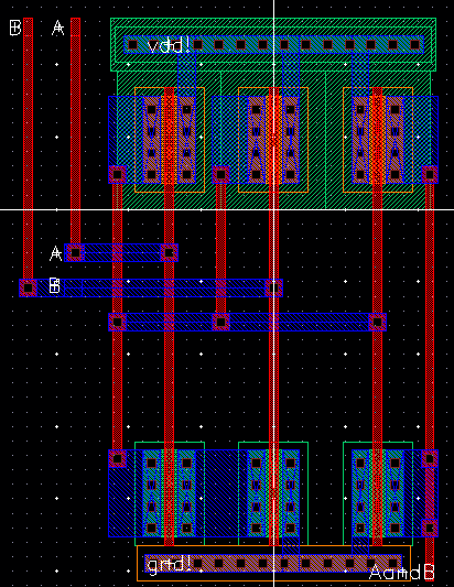
The AND gate
8-bit AND gate layout
The OR gate
8-bit OR gate layout
The Inverter
8-bit Inverter
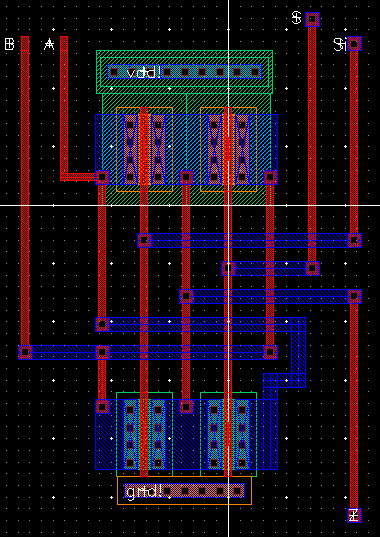
The 2to1 Multiplexer
8-bit 2to1 Multiplexer layout
Note: An inverter was used on the left side of the layout to provide the not(S) signal from the S input.
The Full Adder layout
8-bit Full Adder Layout
Note: The Carry out of stage N is connected to the Carry in of stage in N+1.
The FINAL layout
Note the following:
- The VDD of all the components are routed to the left VDD bus. Metal 2 (higher) is used in order to reduce parasitic capacitance.
- Similarly,
the GND of all the components are routed to the right VDD bus. Metal 2
(higher) is used in order to reduce parasitic capacitance.
- Components area arranged and compacted to ensure small layout area.
- Wire buses are ran all throughout the layout to connect one component to the other.
Overall layout passed all DRC and LVS checks.
Finally, we backed up our design projvi.zip directory and other files for future study.
Return to labs


