Lab 5 - ECE 421L
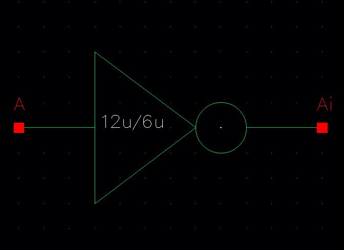
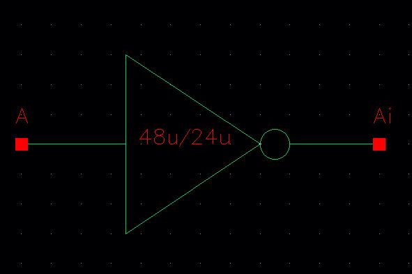
Make sure to check and save the schematic to ensure that there are no errors. To create the symbol go to Create->Cell View-> From Cell View. To create the image below make sure to delete everything except the pins. The inverter symbol is drawn on (Create->Shape->Line). Display the pin names to verify if the pins are in the correct order.
Once you get the proper symbol check and save your work.
Layout:
Add nmos, pmos, ntap, ptap, and m1_ploy to your layout (They can be found in the NCSU_TechLib_ami06 Library)
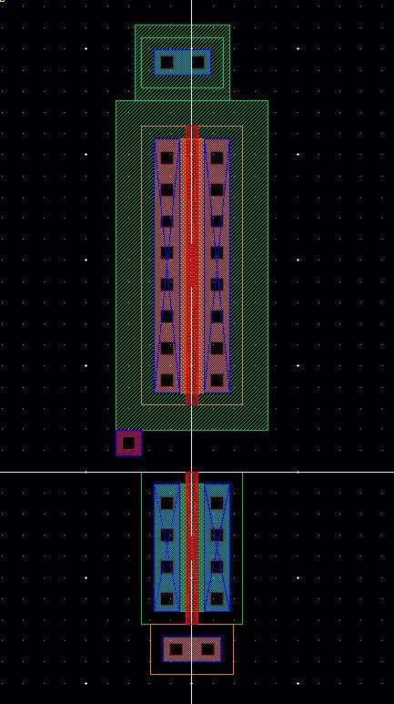
Link the cells using metal1 and insert pin names. Note how an extra poly rectangle was added to connect the input A. Make sure to DRC the layout to verify that there are no errors. Check and Save when completed,
When we have the proper layout, extract the file (Verify->Extract). We need the extracted layout to LVS the system.
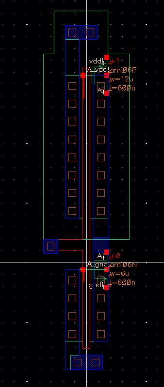
Layout:
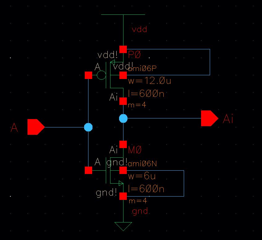
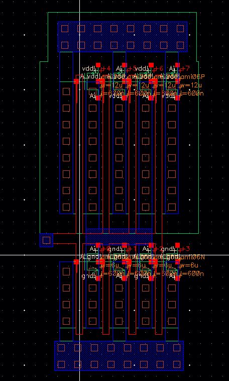
For the second inverter we can copy the same schematic from the first inverter. Pres q (object) to change the multiplier to 4 for both nmos and pmos. We do not change the values for the width and length because the multiplier automatically changes the width to 48u and 24u.
Symbol:
Layout:
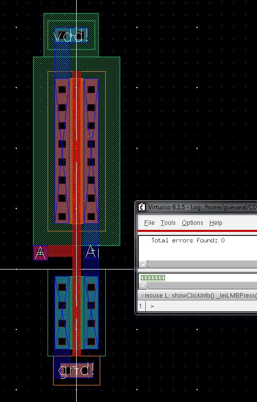
To match the schematic we must change the multiplier value for nmos and pmos. Ensure that everything is connected by increasing the size of ntap and ptap.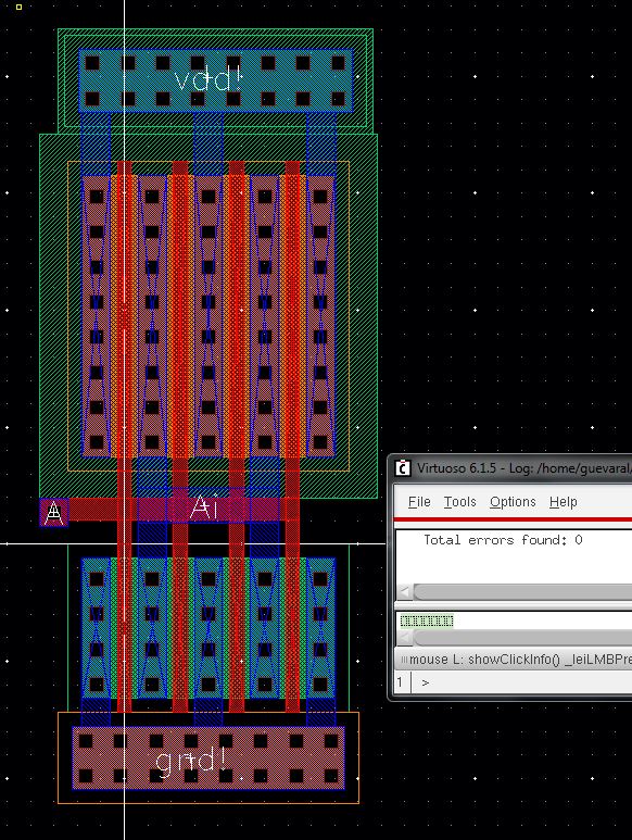
Extracted view:
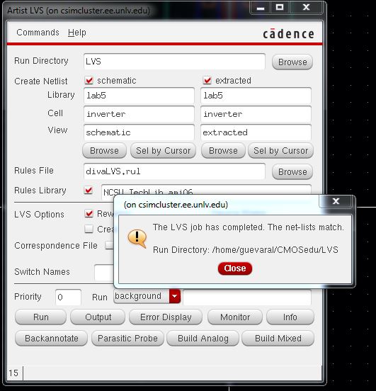
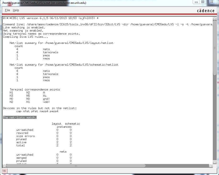
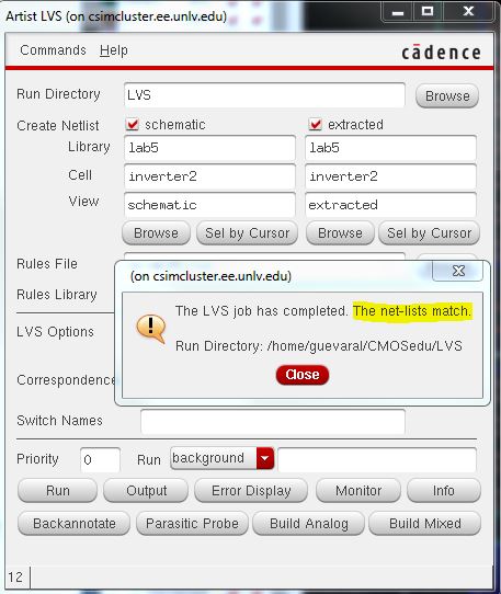
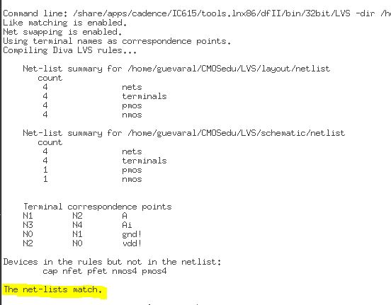
LVS
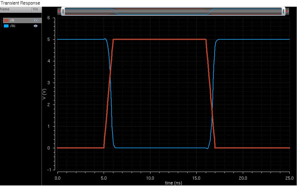
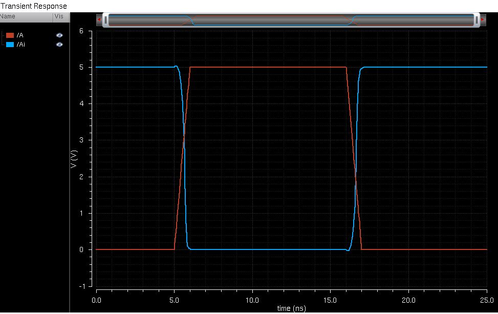
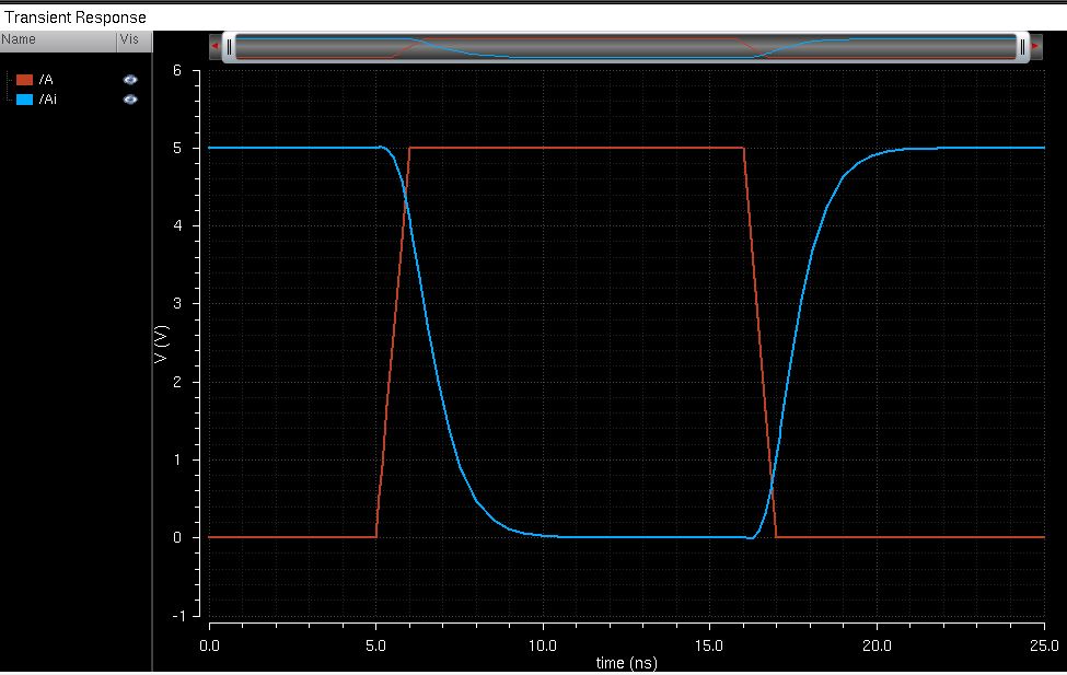
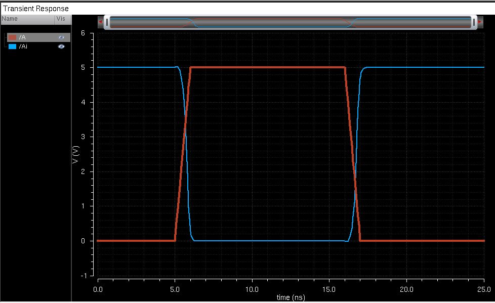
Now that we have both inverters lets run simulations so we can compare differences.
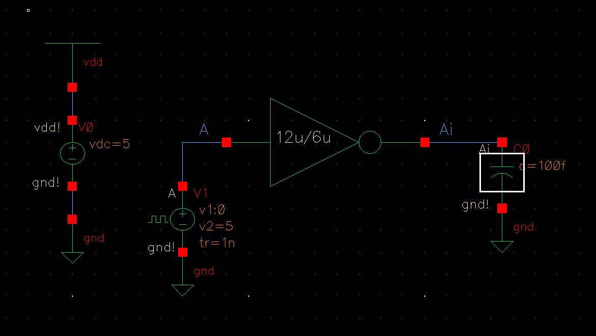
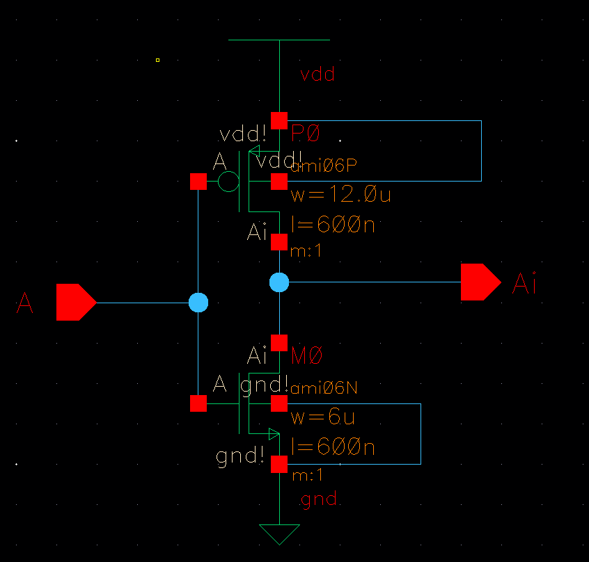
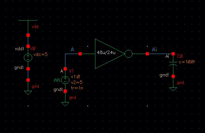
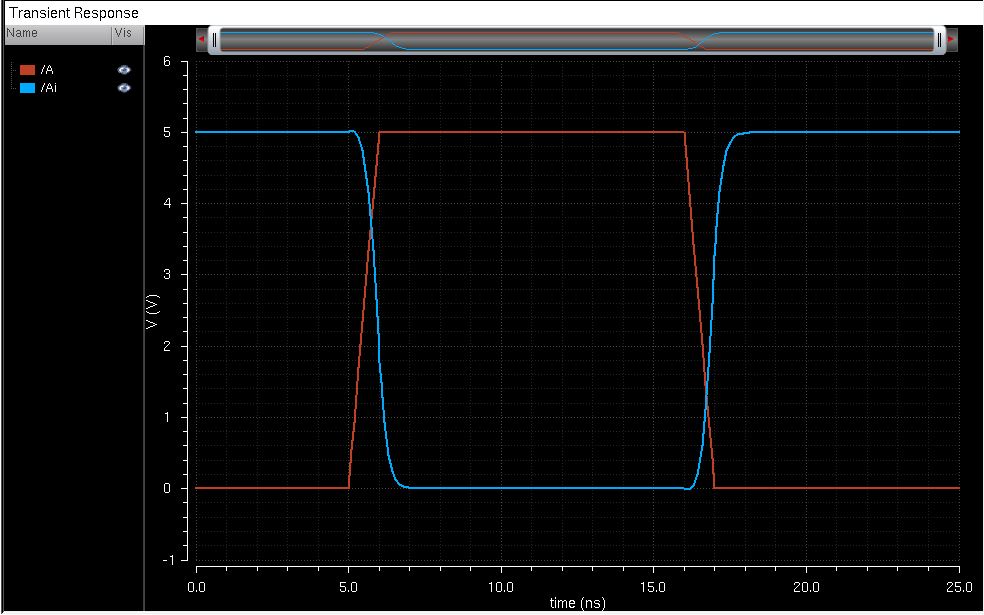
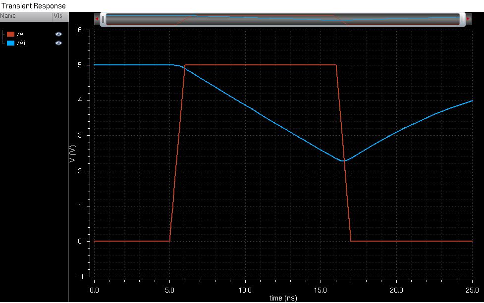
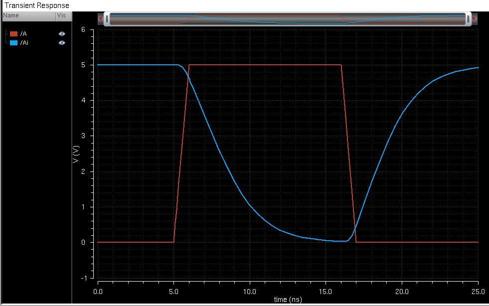
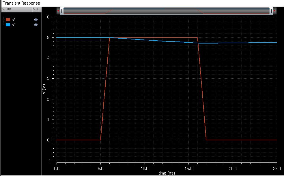
Schematic using the 48u/24u inverter
Setting up the simulations:
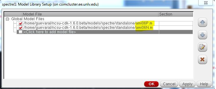
We will be using the ami06P.m and ami06N.m model libraries (Setup->Model Libraries)
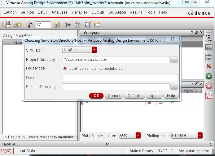
For the labs we have been using spectre state as the standard for the simulations, now we will change the simulator value to UltraSim. UltraSim can only be processed using Transient analysis
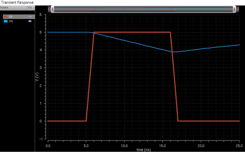
When C=100f F
This ends Lab 5
Remember to zip and email the file to yourself for safe keeping
