Lab 4 - ECE 421L
Authored
by Leanna Guevara, guevaral@unlv.nevada.edu
October 6. 2014
IV Characteristic and layout of NMOS and PMOS devices in ON's C5 process
Before you start the lab, go through Tutorial 2 which talks about laying out the IV curves of PMOS and NMOS devices.
We
will be generating 4 schematics 2 NMOS and 2 PMOS devices. For
additional help and guidance we can look at the CH6_IC61 Library found
in cadence.
NMOS Devices
First
we will create a schematic for a ID v. VDS of an NMOS device. The
instructions want us to set VGS to vary from 0 to 5V in 1V steps while
VDS varies from 0 to 5V in 1mV steps. The width the length ratio will
be set to 6u/600n
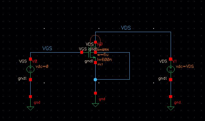
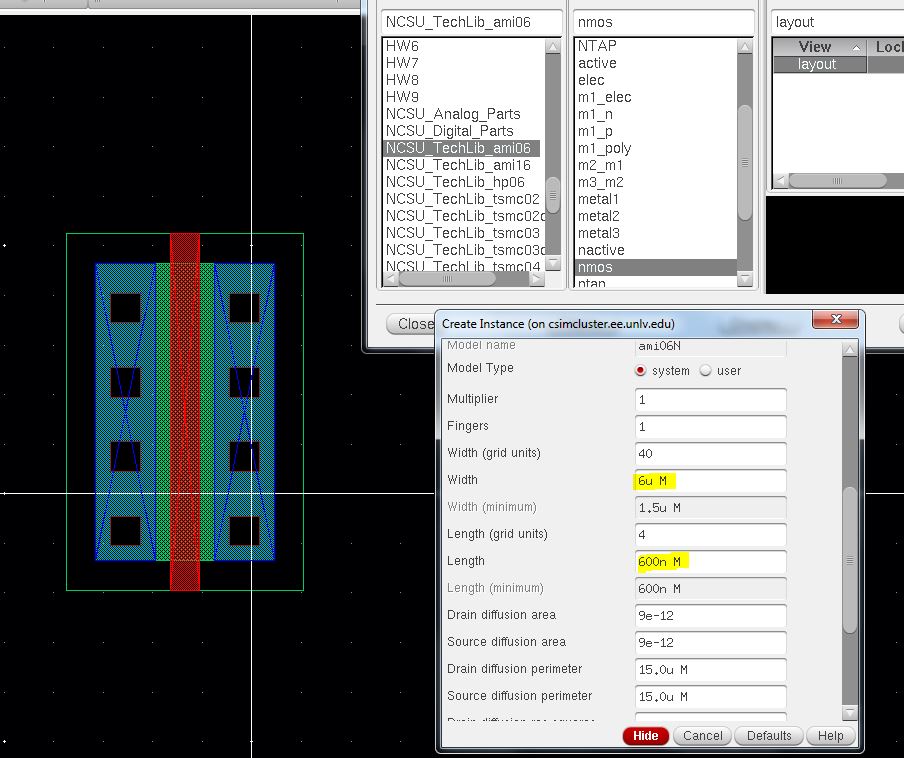
Following the tutorial we will make a symbol for the NMOS. First create the following schematic
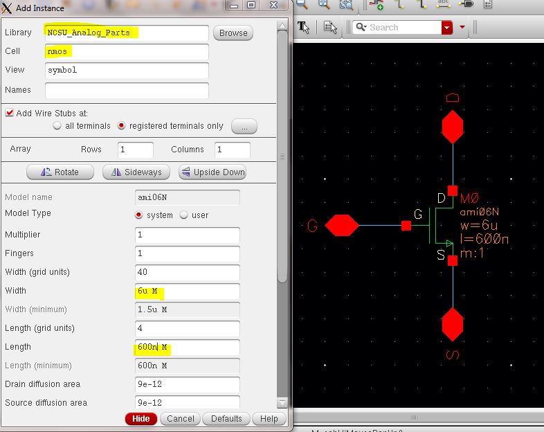
The
nmos device
(Instance->Browse->NSCU_Analog_Parts->N_Transistors->nmos)
is set to a width and length is set to 6u and 600n respectively.
Remember to check and save the schematic.
To create the symbol (Create->Cell View-> From Cell View) set to schematicSymbol and press OK
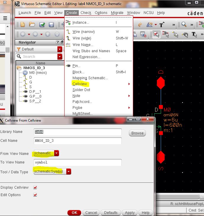
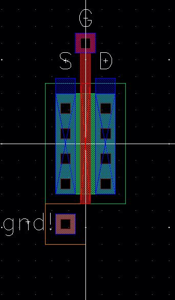
We still have to adjust the look of the symbol to look like
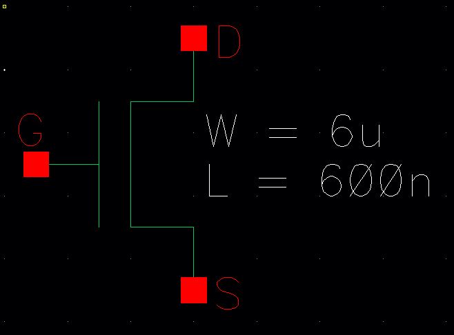
- Delete everything besides pins (You can display pin names by selecting all three pins, open properties and display value).
- Draw the NMOS by going to create->shape->lines.
- The width and lenth text is made by going to Create->Note->Text
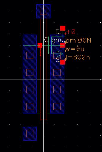
Now we can use the symbol in our NMOS device. Create a new schematic cell view and create the following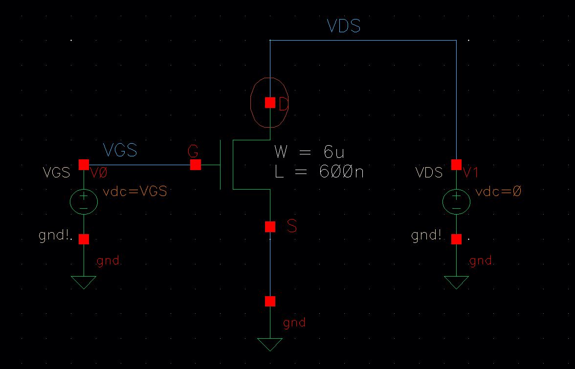
Running
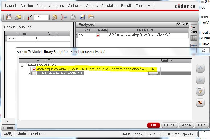
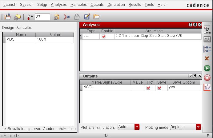
the simulation for this lab will be a little bit different. First
launch the ADE L. Open the Model library (Setup->Model
libraries) by clicking the button with three periods we can browse the
libraries. Look for the highlighted model file (Note ami06N.m refers to
NMOS, for PMOS we will use ami06P.m). Press OK
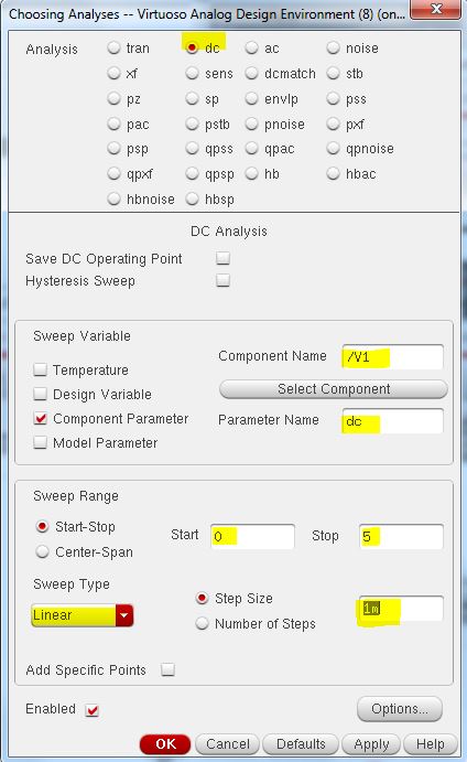
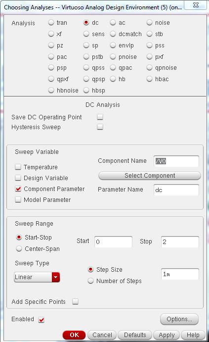
We now set the DC Analysis. This is where we will set the VDS values.
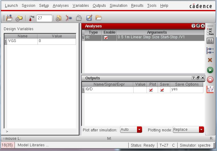
This is what the ADE L should look like (Note that the variable VGS was set to 0 and we will be plotting the current at the D)
Usually
at this point we would just run the simulations, since we want to plot
different values of VGS we will have to do a Parametric Analysis
(Tools->Parametric Analysis)
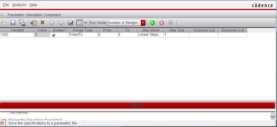
- Set VGS from 0 to 5V
- Step mode: Linear Steps
- Step size: 1
- press the green play button to run
If everything runs smoothly the following graph should appear
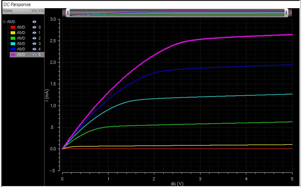
Now we can create the second NMOS Device.
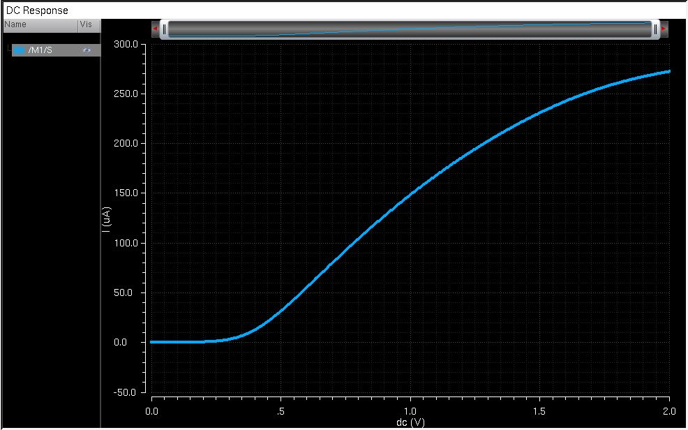
The
lab wants us to simulate ID v. VGS when VDS=100mV and VGS varies from 0
to 2V in 1mV steps. We will be using the same length and with ratio as
the last device.
Create the following schematic (Note that this time we use the nmos4 symbol)
Once
the schematic has been checked and saved open up ADE L for the
simulation. When setting up the DC analysis we will set the range for
VGS.
ADE L should look like
Since VDS is a set value we do not need to do a parametric analysis. We can run the simulation as usual.
PMOS Device
The
lab wants us to create a schematic to simulate ID v. VSD for a PMOS
device. The instructions state to set VSG from 0 to 5V in 1V steps and
set VSD from 0 to 5V in 1mV steps (Note that there are two ranges so we
will be doing a paramentric analysis again). The length and with shall
be set to 12u and 600n respectively
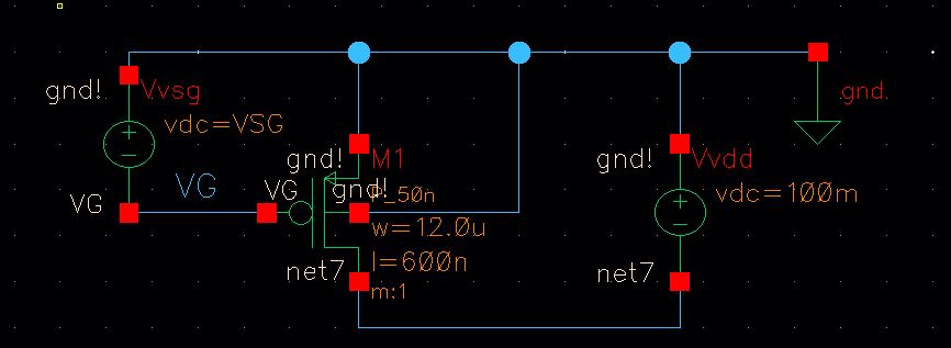
The schematic
Just like the first device we created a new symbol for the pmos, this time we have 4 pins instead of 3.
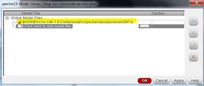
Make sure to add the PMOS library file in the Model Library
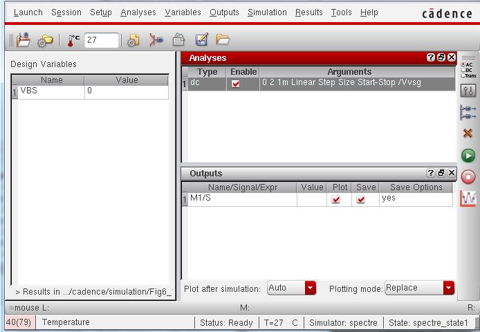
The ADE L window should look like
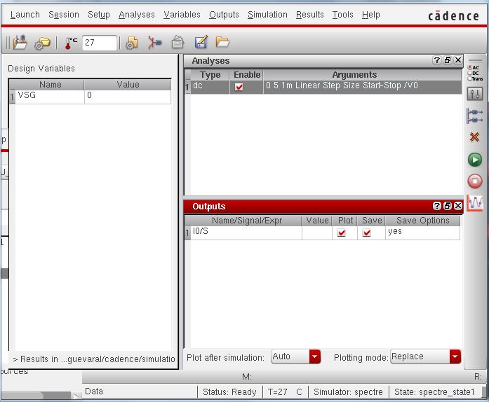
- For the DC Analysis we will set the range for VSD (Range from 0 to 5 with a linear step size at 1mV)
- The variable VSG is set to 0
Now open up the Parametric Analysis (Tools->Parametric Analysis) and set VGS as follows
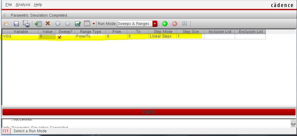
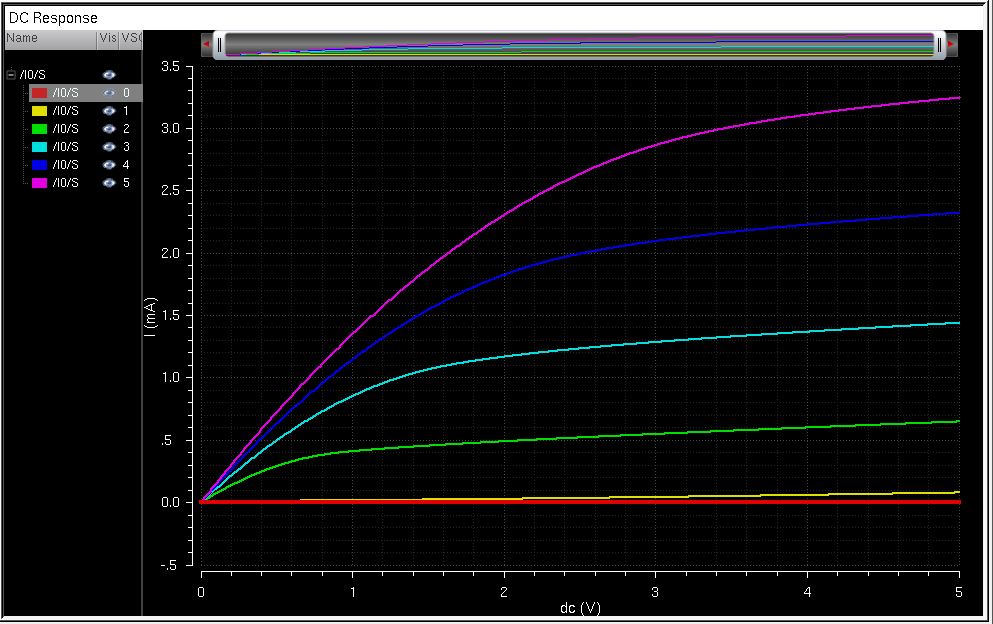
After running the simulation the following graph should appear
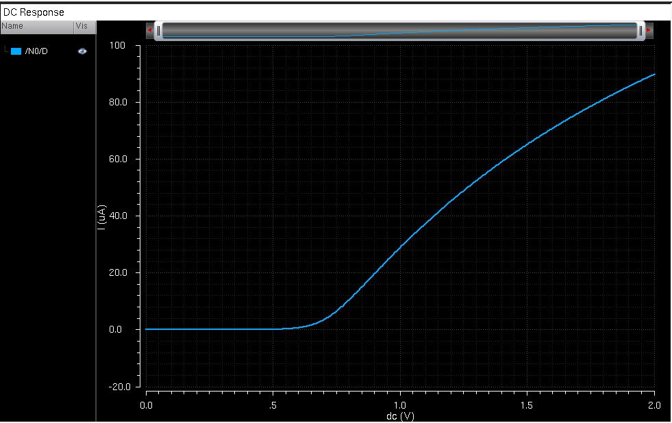
For
the second PMOS device the lab requires that we simulate ID v. VSG when
VSD=100mV and VSG ranges from 0 to 2 V in 1mV steps. We will be using
the same width and length ratio as before. (Note since VSD is given we
will not be doing a parametric analysis)
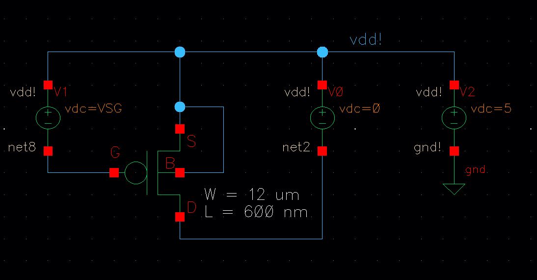
The schematic
For this device we will not be creating a new symbol from instance we used pmos4.
Once the schematic is built open up ADE L and copy the following
When simulating the graph we get
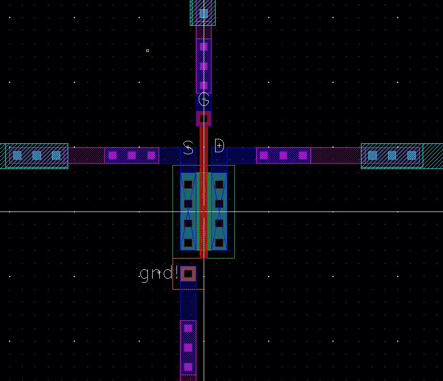
The next part of the lab wants us to layout a 6u/0.6u NMOS device and connect all 4 MOSFET terminal probe pads
First lets instantiate a NMOS device that is 6 um wide and 600nm long.
We want the layout to look like
On the layout
- ptap
- metal1 to poly (m1_poly)
- poly rectangle (used to connect the NMOS to m1_poly, there will be an error if they are too close together)
- Use metal1 to draw rectangles for the drain and the substrate
- Add the pins for gnd!, S, D, and G
Make sure to DRC the layout to ensure that there are no errors. If there are no errors extract the layout (Verify->Extract)
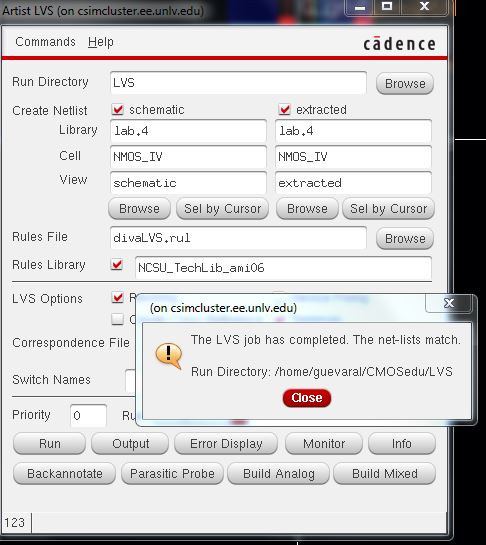
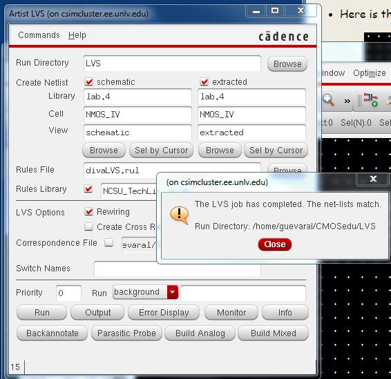
If
you try to LVS (Verify->LVS) the extracted view with the NMOS
schematic from the beginning there will be an error. In order for the
extracted view and the schematic to match we must turn the 3 terminal
transistor to a 4 terminal transistor.
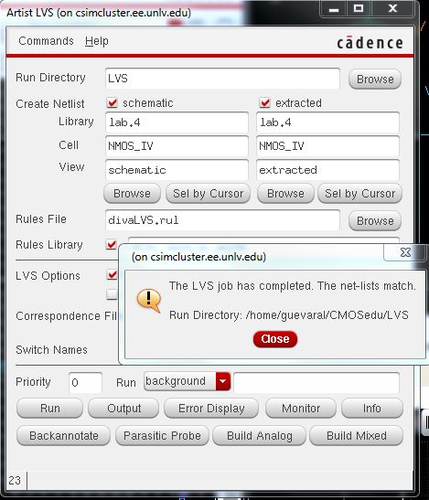
So now when we LVS the schematic and the extracted view the netlist should match
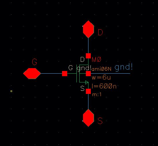
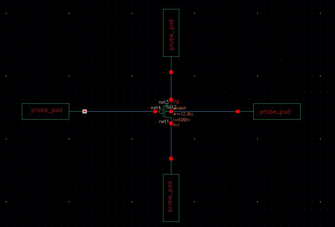
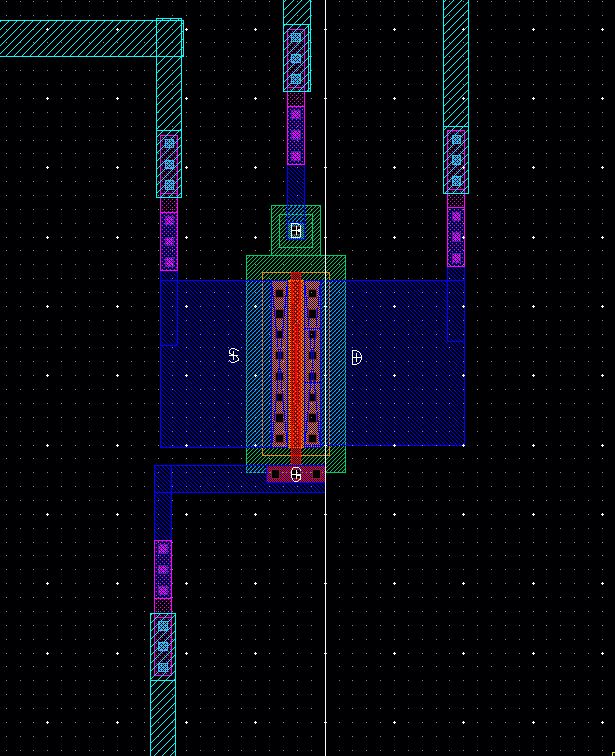
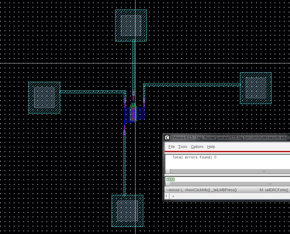
Now that we have the correct NMOS device lets connect the 4 MOSFET terminals to the probe pads
Schematic
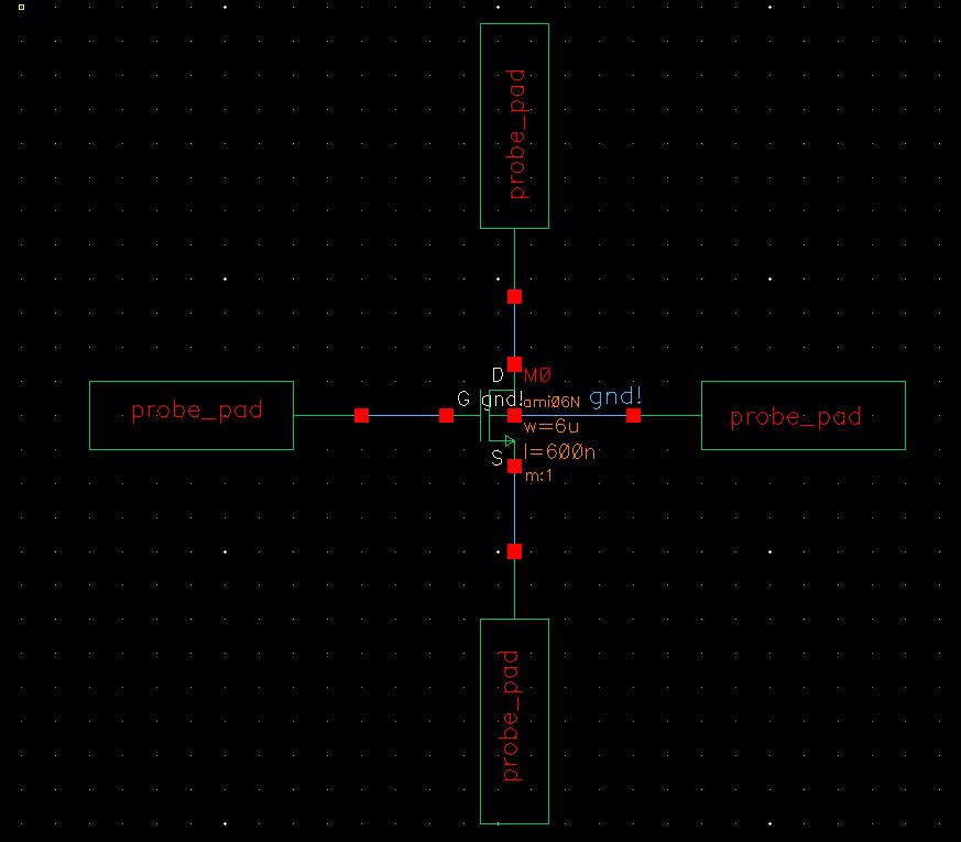
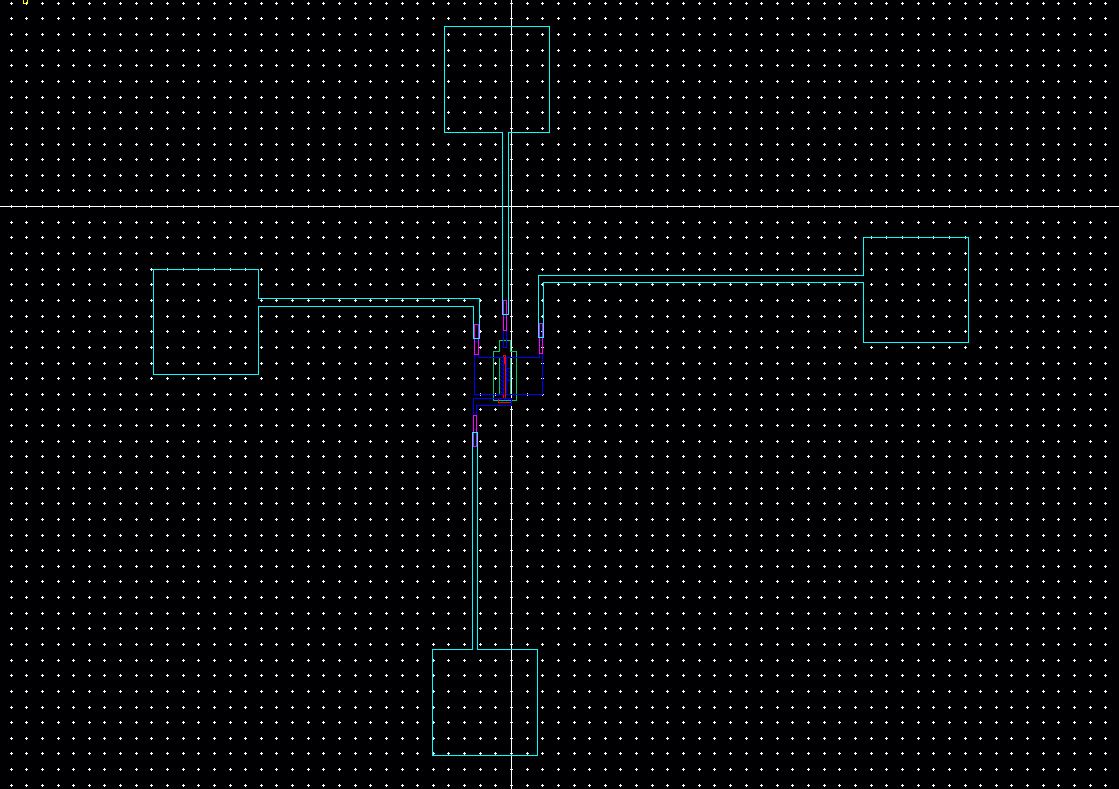
Layout
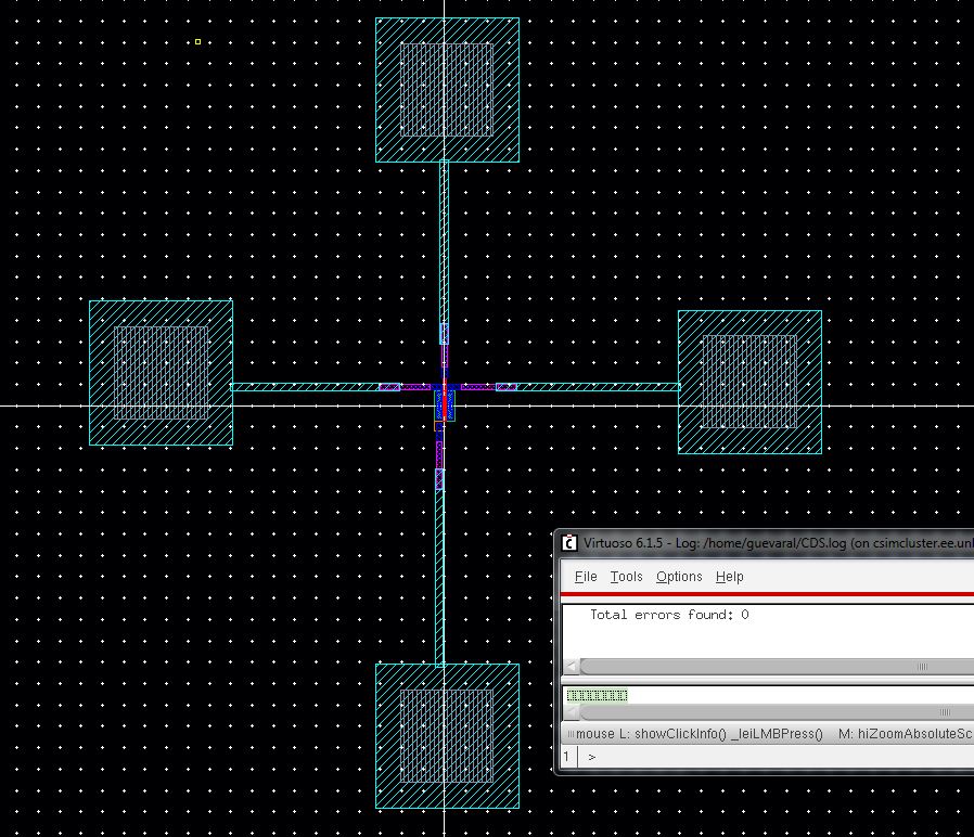
Zoomed in
LVS the layout and the schematic to make sure they match
Next lets layout 12u/0.6u PMOS device and connect all 4 MOSFET terminals to the probe pads
Schematic
Layout
Extracted
LVS
This is the end of Lab 4
Remember to zip the Lab 4 file and email to yourself for safe keeping
Return to EE 421 Labs