EE
421L Digital Integrated Circuit Design - Lab 7
Using
buses and arrays in the design of word inverters, muxes, and high-speed
adders
Author: Abel De La Torre
Octover 31th, 2014
delatorr@unlv.nevada.edu
Pre-lab
work
- Back-up all of your
work from the lab and the course.
- Go through Tutorial 5 seen here.
- Read through the entire lab before starting it.
Wide wires (buses) are added using the bindkey shift+W or the menu button seen circled below.
Arrayed symbols (by changing
the symbol's name) are used to make schematics concise and
easier to use.
4 bit inverter:
Below is the schematic of an inverter which will be later used for a 4 bit inverter

Now with the previews schematic we create a schematic for a 4 bit inverter.

Finally we can create a symbol for the coresponding inverter schematic. Now we have a symbol we can use.

The following schematic is used to test the 4 bit inverter . The inverter is connected to 3 capaxitors. Using this symbol create a simulation
schematic like the one seen below. All four inverters' inputs are tied together to an input pulse source.

This schematic displays the 4 separate inverters that will be tested and simulated.

The following displays the inputs and output of the four independent capacitance loads from the previews schematic. The capacitive loads influence the rise and fall times of the inverters outputs by slowing the rise and fall time of the output. The output is slowed to a gentle slope for rises and falls. The larger the capcitance, the longer it takes for the rise and fall slopes to reach their plateau.

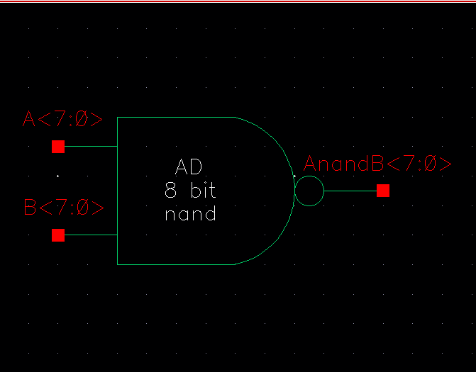
8 bit NAND Gate:
We now create a circuit schematic for a nand gate which will alos be used later in this lab

The following is the 8 bit nand gate schematic of the corresponding previewsly displayed

Now, we create the nand symbol of the corresponding schematic.
In the same manner a test schematic is created to test the 8 bit nand gate.

After simulating the test schematic for the 8 bit gate the output is displayed below. all output are high for every bit case except when both inputs are high.

8 Bit NOR Gate:
Now, the same procedure its follow to create an 8bit Nor gate . The following display the coresponding schematic for the OR gate.

After the previews schematics now a symbol is created for the OR gate

And we can also create a test schematic to simulate the gate and come up with our desired output.

The following displays the outputs of the Nor gate showing a high output when inputs are low.

8 Bit AND Gate:
Now an 8 bit AND gate is circuit schematic is created


A symbol for the previews schematic of the AND gate is created and shown below.

Now, a test schematic is created to test the circuit by simulating the AND gate

This is the output dislplay of the AND gate showing the output high when both inputs are high.

8 bit inverter:
Now, we pick back up from the previews 4bit interter and we create an 8 bit inverter as it was done at the start of this lab.

An 8bit inverter symbol is created and shown below

As we have been doing, we now create a test schemtic with the 8bit inverter and we get ready to simulate .

After simulating the test schematic, the following displays the output and we can see how it is the inverse of the input.

8 bit OR:
Now we create an 8bit OR gate and the circuit schematic is displayed below.
Similarly, we create a schematic using the 8bit OR gate shown below.

This is the corresponding symbol for the or gate.

And again, we create yet another test schematic for the 8bit OR gate and we get ready to simulate.

The following waveform shows the output display of the 8bit OR gate shown that when 1 input is high the output is high.

2-1 MUX:
Create an 8-bit wide word 2-to-1 DEMUX/MUX schematic and symbol.Include an inverter in your design so the cell only needs one select input, S (the complement, Si, is generated using an inverter).
Use simulations to verify the operation of your design.
The following shows the circuit schematic for the 2 - 1 mux.

The following is the symbol for a 2-1 mux

The following shows the output waveform showing that when S is low the output is the trace of B and when S is high the output is A.

2-1 DEMUX:
Like the mux now a demux is created which is the inverse of the mux. The following shows the schematic for the demux.

A symbol is created and shown below for the 2-1 demux.

The following is th eshematic for the 8 bit mux
 The symbol below is created for the 2-1 8 bit mux.
Test circuit shown below used to simulate the 2 -1 8bit mux.

The following displays the output for all 8 bits of the 8 bit 2-1 mux.

8 bit Demux:
The following shows the schematic for the 8bit 2-1 Demux. The symbol below is created for 8 bit 2-1 demux.
This is now the test circuit schematic for the 8 bit 2-1 demux.

The following shows the 8 outputs coresponding to the 8bit 2-1 demux.

ADDER:
Now we create the Full Adder. The following shows the schematic of the full adder. The following is the created symbol for one section single full adder.
 The following schematic is created to test one section a single individual part of the full adder.
The following is the output of the schematic for one single adder. It shows S high when theres only one high input and when theres 2 high inputs Cout = high. and S=low. When all inputs are high, S=Cout= high.

8 Bit Adder:
Now we create the 8bit Adder using just one single adder schematic.

This is the symbol for the adder.

Now a test circuit schematic is created just like the others to simulate and test the output. 2 8 bit numbers will be added with cin being applied.
Here is the testing schematic for this adder. Here, we will be adding 01101010 and 10110101 with an external cin coming in.
 Along with the Cin, the
total is 100100000. Our output has only has Cout high, and
out<5>
high, indicating a correct output.
Along with the Cin, the
total is 100100000. Our output has only has Cout high, and
out<5>
high, indicating a correct output.The following 2 schematic are split into 2 to show both inputs and outputs. below is the simulation of the following calculation inputs.
The sum calculation is: 1 1 1 1 1 0 1 0
0 0 1 1 0 1 1 0
0 1 1 0 0 0 0

This
is the simulation waveform for the outputs. As you can see it
matches the output calulated in the above sum prediction.

Full Adder:
Finally, we can layout the full adder. We start with one single unit of the 8 bit adder shown below. After its layed out it is DRC to check for errors.

The following is the extracted view of all 8 units of the 8 bit full adder

The Layout is then LVS to test schematic vs extracted and the full adder shows a net list match.

Create Backup:
We now compress the lab 7 folder into a zip file.
Email the Zip file to your self to secure the data

These cells are located in directory call lab7_AD.zip