![]()
Lab
Project - ECE 421L
Authored
by Jeevake Attapattu,
attapatt@unlv.nevada.edu
11/19/2014
Simulation and layout of an ALU with AND, OR, ADD, SUB
Using MobaXTerm log into csimcluster.ee.unlv.edu.
The
first action is creating a backup. Type tar -cvf "date"CMOSedu.tar
CMOSedu/. This will create a tar file
with all the project and homework saved. In place of "date" type in the
date creating the backup. Unce the backup has been created type gzip "date"CMOSedu.tar.tar. This will
create a .tar.gz file witch is significantly smaller.
Use
MobaXTerm to download the file to your own pc then upload to a backup
site such as dropbox or google drive.
Launch Virtuoso.
You will be using
previous work from the
tutorials.
Download all
tutorials if needed from here.
You
will need the cell views created in lab 7. Specifically the 8 bit adder, inverter, and gate, or gate, and 2-1 mux.
The first step of creating the alu is to figure out how all the
operations are done. The and
and or
operations are straight forward. The adder can be used without any
modification for the add
operation. The sub
operation requires more thought. One method of creating a substractor
is by using an adder and 2's complement. Since we will be using A-B, B
would need to be turned in to 2's complement form and added to A.
To
create a 2's complement the bits need to be inverted and added to 1.
This can be implemented with a carry in and an inverter.
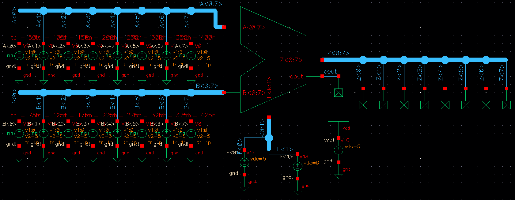
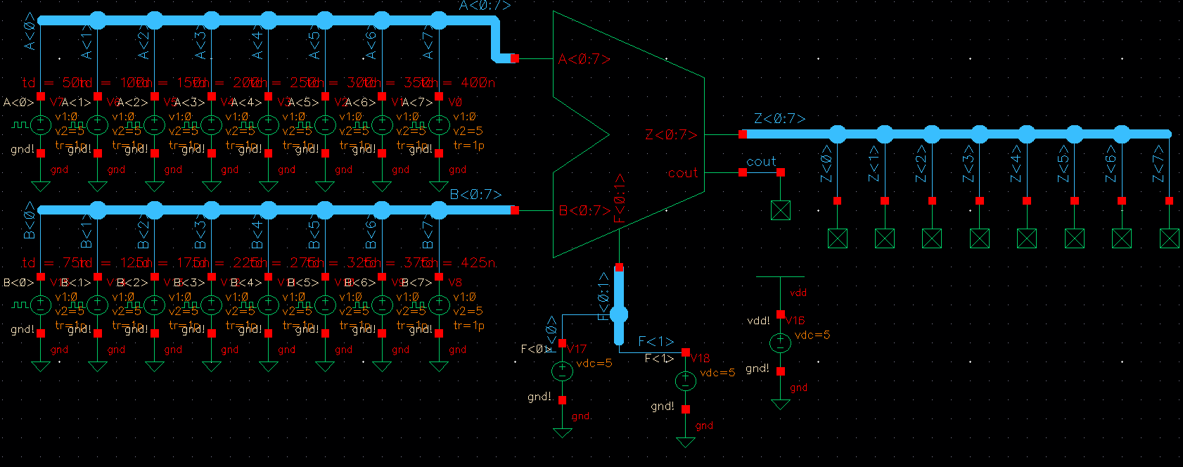
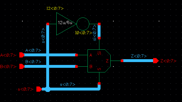
The image below is my schematic.
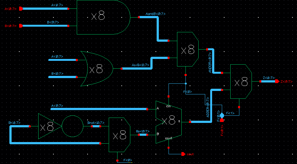
The way I have set up my schematic the control signal is F. 00 is A+B, 01 is A-B, 10
is OR, and
11 is AND. Feel free to set up your
own control signals if necessary. Next create the symbol.
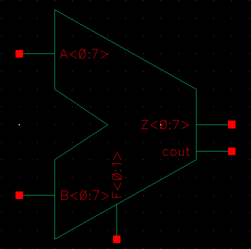
You can change the symbol and schematic so that F is and array.
Now let's do some simulations. We will begin with the A+B
simulation. I chose to use a 8 pulse inputs for each input. This method
allows me to observe mutiple cases with one simulation. I have used
voltage sources to avoid shorting issues. If you use this method for
this simulation set the dc voltage to 0V.
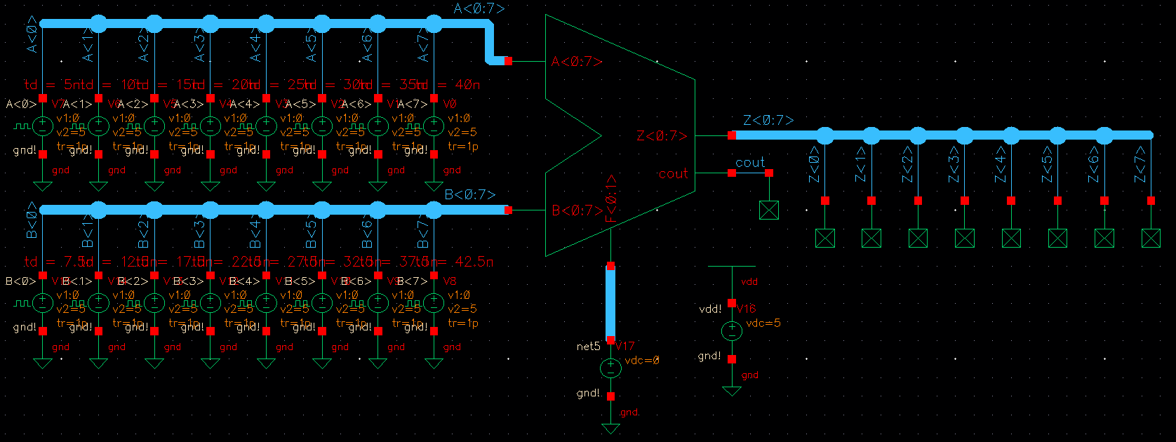
Open
ADE-L and plot the circuit. When selecting inputs to be
plotted
it can save time by selecting the arrays on the left of the schematic
window. Your plot should have 25 traces. Split the graph by trace to
get a better look. Below is the graph I have plotted.
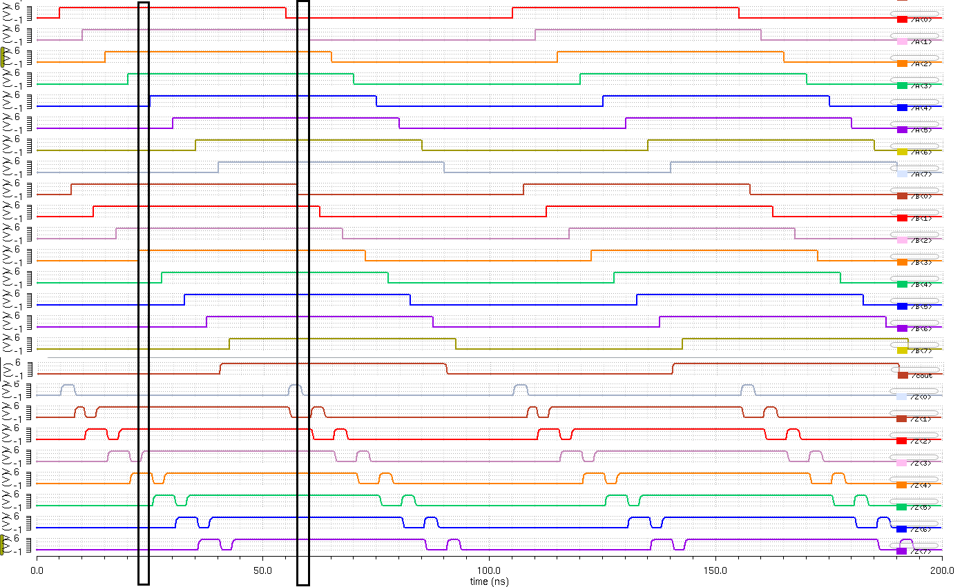
Lets
look at a couple of points selected at random. The first point has
A=15, B=15, and Z=30. This is what we expect. Cout is 0 since there is
no carry out. The secong point is A=254, B=254, and Z=252. This doesn't
appear correct untill you look at the carry out. Cout is 1, which means
that A+B=508. Again this is what we expect.
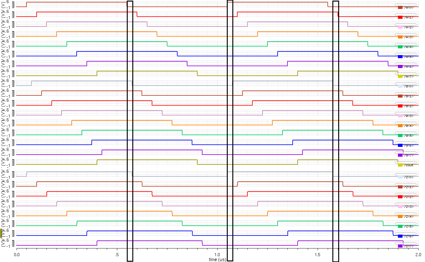
Next lets try the A-B
simulation. Notice the shape of the output wave forms. This tells us
that the ALU is too slow for the signals we are looking at. If this
happens increase your pulse width and period. Copy the A+B schematic to
a new cell. This time you will have to split F into components.
Use array labels on the wires to control which is which. Set F0 dc voltage to 5V
and F1 to
0V.
Plot
the results in ADE-L. I have changed the line thickness to medium and
the style to solid to make it clearer. This time lets look at three
sets of numbers.
The first one has A=63, B=31, and
Z=32. Ignore the cout as it is an overflow bit. The second one has
A=240, B=248, and Z=248. This doesn't seem right. Look at cout. The 0
idicates a negative number. 2's complement of 248 is 8, which is what
we expect. The third one has A=255, B=127, and Z=128. Once again the
cout is an overflow bit.
Next is the OR
simulation. To save time simply copy the A-B simulation and interchange
the voltages on F0
and F1.
Make sure that you update the instances of the copy. If you do not the
simulation from ADE-L will point to the previous schematic.
The save the changes before you plot. Open the saved state from the
library manager and hit run.
Let's
look at a few regions. Since this is a bitwise operation we do not have
to convert binary to decimal. The first is A = 11111110, B = 11111111,
and Z = 11111111. This is what we expect. Let's look at the second
region A = 00000001, B = 00000000, and Z = 00000001. Again this is what
we expect. Look at the last region. Here A = 11111110, B =
11111110, and Z = 11111110. Another expected result. You can choose a
few more at your own convinience.
Next
is the AND
simulation. To save time simply copy the A-B simulation and change the
voltages on F0
and F1 to
5V. Make sure that you update the instances of the copy.
The
save the changes before you plot. Open the saved state from the library
manager and hit run.
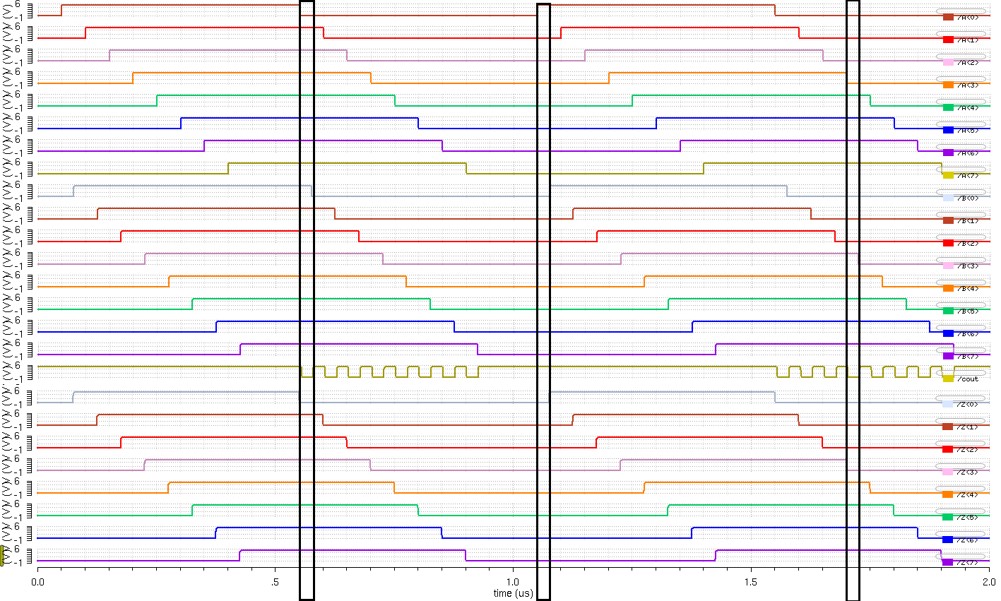
Let's
look at a few regions.
Again, since this is a bitwise operation we do not have to convert
binary to
decimal. The first is A = 11111110, B = 11111111, and Z = 11111110.
This is what we expect. Let's look at the second region A = 00000001, B
= 00000000, and Z = 00000000. Again this is what we expect. Look at the
last region. Here A = 11110000, B =
11111000, and Z = 11110000. Another expected result.
It
should be noted that for both the OR and AND operations cout still
outputs a value. The carry out should be ignored for these operations
since they do not use the adder.
That
concludes the first part of this project. Here
is the design directory used in this lab.
Part 2 -The layouts
The second is to create the 8bit layoutsThere are 2 methods of laying
out the 8bit ALU. The first method is to create 1bit alu with
the
one bit components and join them together. of the components and join
them together. I have chosen the second method.
Let's
begin with the 8bit inverter. If required refer back to lab 7 for
arrays and buses. The first step is to add the idividual pins as
arrays. The second step is to connect the vdd!s and gnd!s with another vdd! and gnd!. There is
some overlap between the n-well layers for compactness and eliminating
DRC errors.
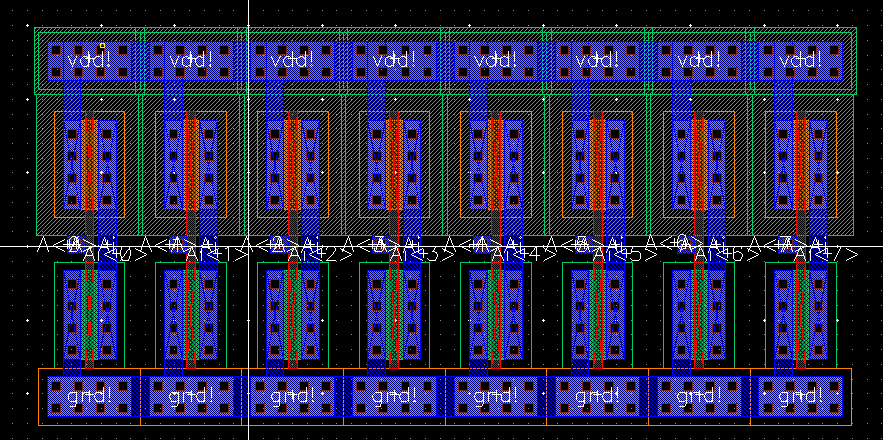
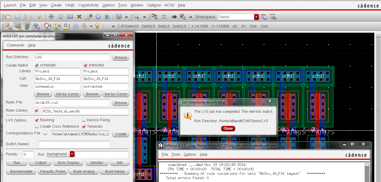
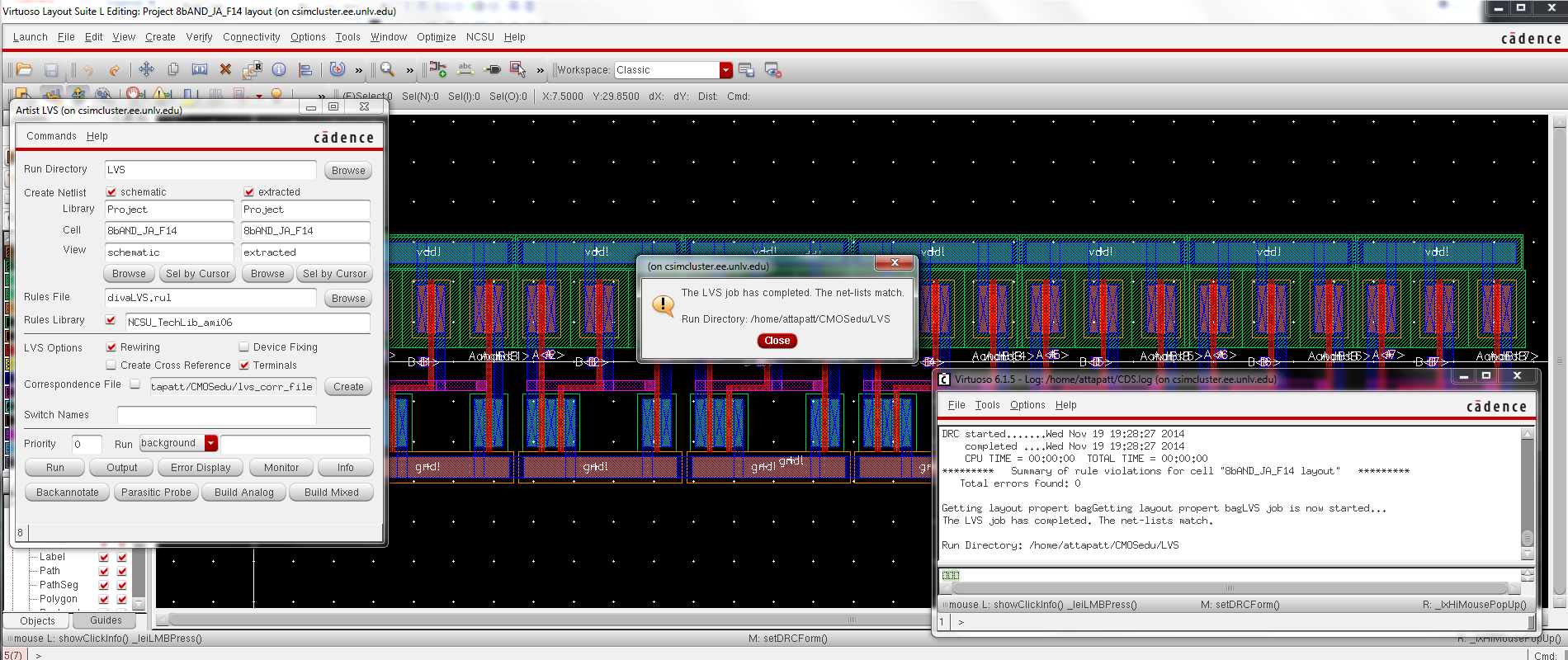
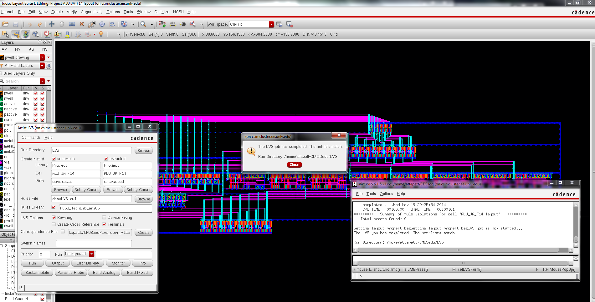
DRC and LVS the layout.
Repeat the procedure for the AND gate.
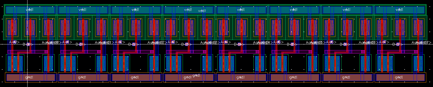
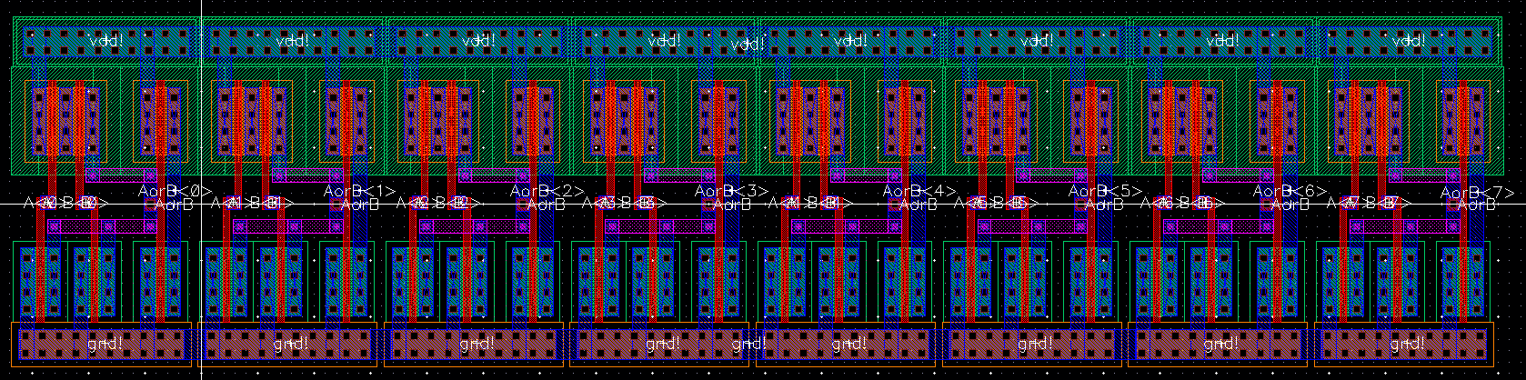
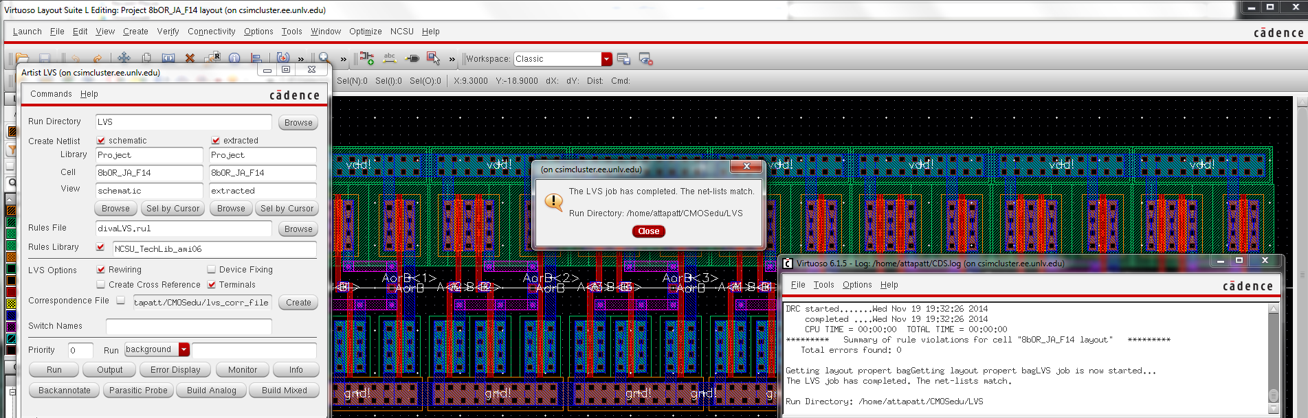
Repeat the
procedure for the OR gate.
The
mux is slightly more complecated. The addition of the inverter means an
extra component in the layout. I refering to the schematic I have
chosen a 12u/6u inverter becuase of the vdd/2 switching point.
Since
we did not create the mux layout in before, this one needs to be
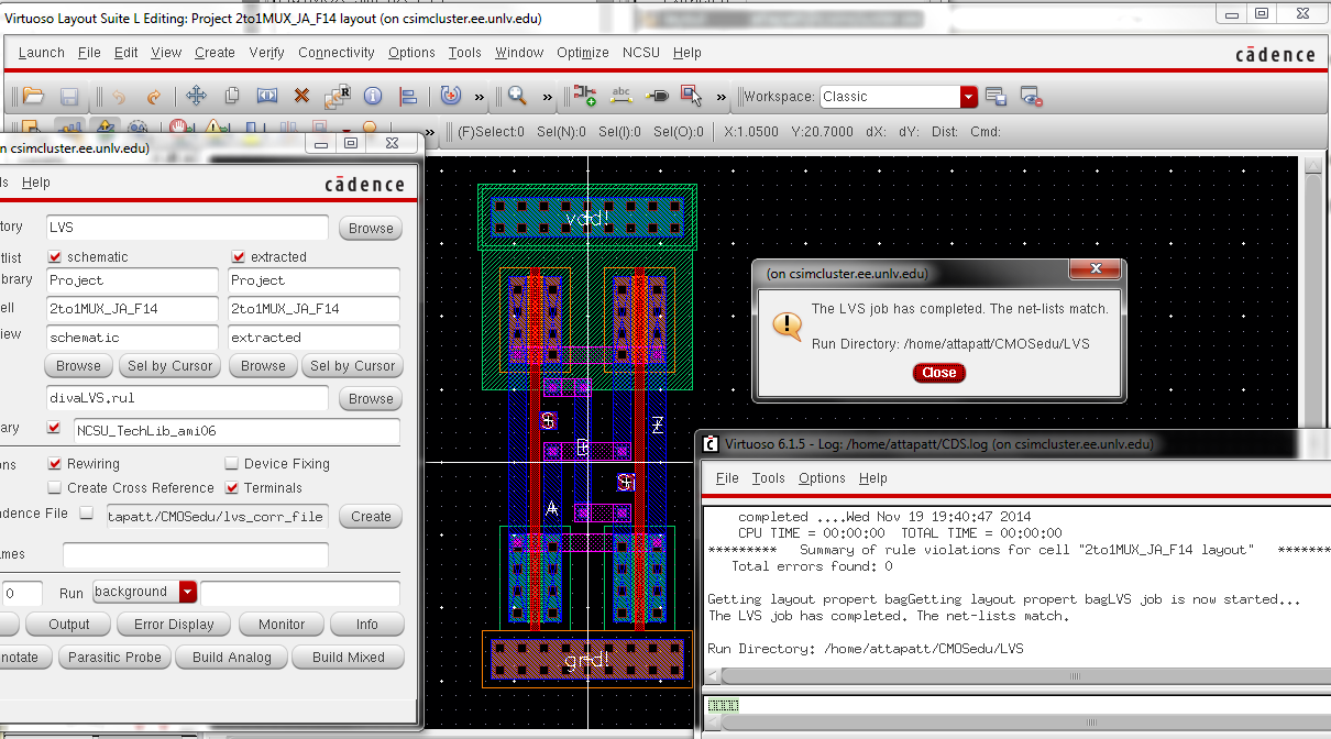
created. Follow the layout below and DRC and LVS it. It is important to
catch errors early on so that you do not have to jump back and forth
trouble shooting components.
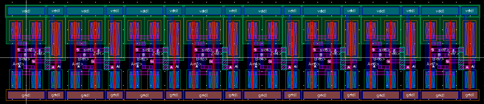
Now
create the 8bit mux. Remember to add the inverter. I have used metal3
to connect the S and the input of the inverter. And metal 2 is used to
connect the output of the inverter and S'. I kept the individaul S
inputs for bitwise selection if necessary.
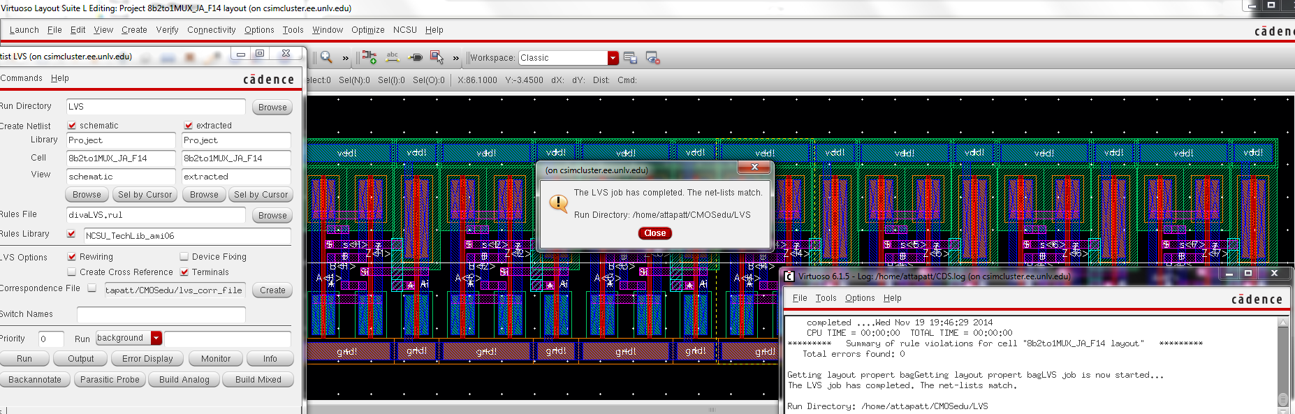
DRC and LVS the layout.
Next is the 8bit full adder. We have already compeleted the adder in
lab 7.

Now let's move on to the ALU layout.
My layout is the image below. Click on it for a larger view. The far
metal1 layers on the left are to connect the gnd!s. The ones on
the right are for the vdd!s. The Z bit contacts are placed on the bottom mux. The cout is still on the adder.
href="http://cmosedu.com/jbaker/courses/ee421L/f14/students/attapatt/proj/21b8alu20.0w.png">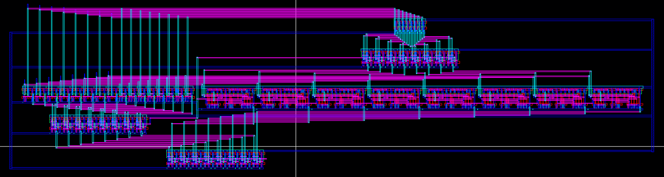
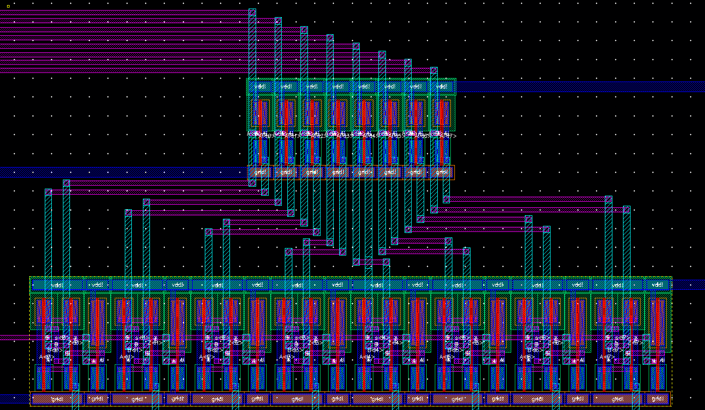
The
components on the top right are the inveter and adder used for the 2's
complement sent to the full adder. I tried to stay with the convention
where metal1 and metal3 are used for vertical connections and metal2 is
for horizontal connections. Becareful as below where the metal3 layers
need to connect to pins. If they connecto to metal2 use m3_m2 from the NCSU TechLib ami06.
If connecting to metal1, add m2_m1.
If connecting to poly add m1_poly.
This is why I try to connect metal3 to metal2 layers in the components.
It is vey easy to miss a few connections. If you LVS and have too many
nets this is a possible cause.
Next lets look at the AND
and OR
gates. Notice the input A pins. They are connected to the metal2 bus
since the AND gate, OR gate, and adder use it. You can see how the bus
extends futher right since it has to reach the adder. The B inputs are
further up since it needs to go to the inverter and mux in the image
above. Notice the F bit next to the mux at the bottom of the image.
Also remember to connect the S pins in the mux's since we will not be
using bitwise selection.
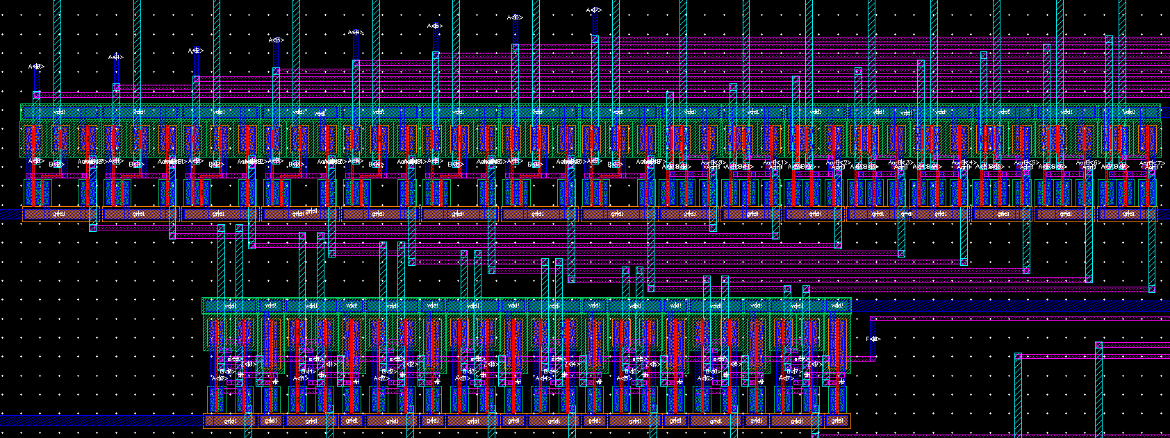
Finally DRC and LVS the layout.
This concludes
the second part of this project. Here
is the updated design directory used in this lab.
Return
to EE 421L Labs
