Lab 07 - ECE 421L
Authored
by Jeevake Attapattu,
attapatt@unlv.nevada.edu
10/25/2014
Simulation and layout of a Full Adder using NAND and XOR gates
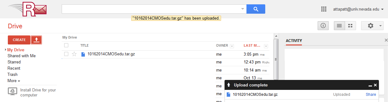
Using MobaXTerm log into csimcluster.ee.unlv.edu. The first action is creating a backup. Type tar -cvf "date"CMOSedu.tar CMOSedu/. This will create a tar file
with all the project and homework saved. In place of "date" type in the
date creating the backup. Unce the backup has been created type gzip "date"CMOSedu.tar.tar. This will create a .tar.gz file witch is significantly smaller.
Use MobaXTerm to download the file to your own pc then upload to a backup site such as dropbox or google drive.
Launch Virtuoso.
You will be using previous work from tutorial 5.
Download all tutorials if needed from here.
In the library manager copy the files in lab 6 to lab 7.
Make sure that you update intances when copying.
Open
a new layout called pad since we are going to create a pad.
Start with the pad layer. The pad layer is going to be used later for
alignment purposes. According to the tutorial we need to use a
120umx120um pad.
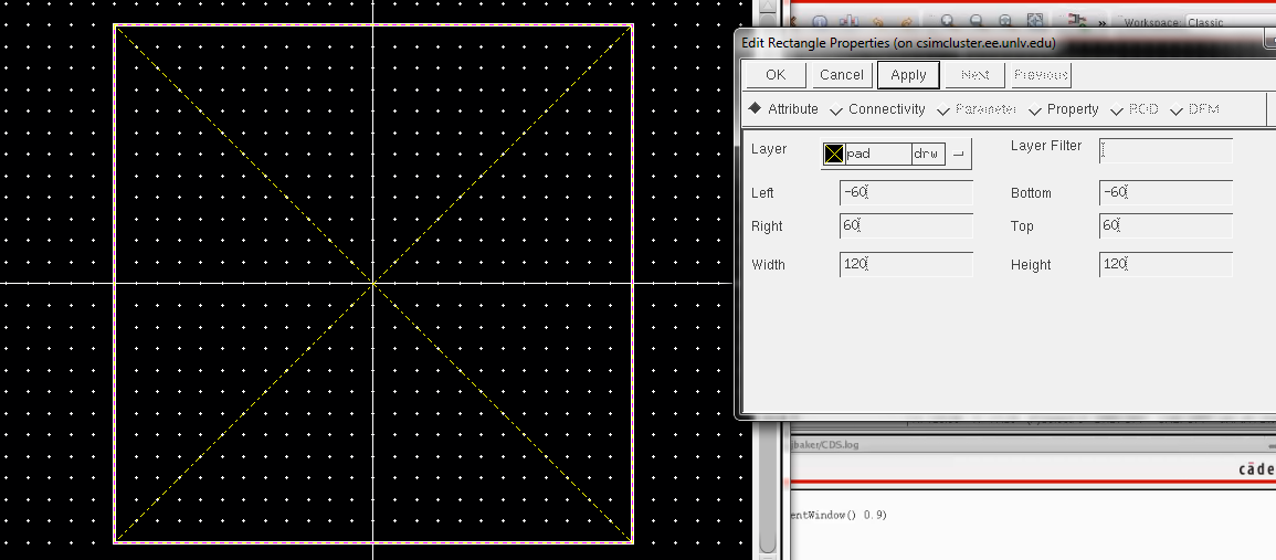
Use a 75umx75um metal 3 layer and
an overglass layer of 63umx63um. Notice that 75-63=12. That is 6um on
each side which is specified by the MOSIS design rules.
The last component is to add a pin on metal 3. Make sure that it is inputoutput and name it pad. Select the text and change the height. I chose 16.
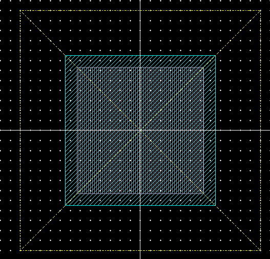
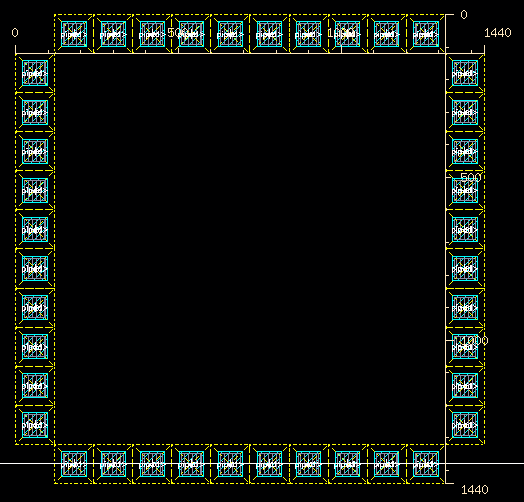
Next create a new layout called pad frame. Type i and place an instance of the pad you just created. Place another metal 3 inputoutput pin on top. Call it pin<1>. This notation is to indicate an array. Use c
to copy and select 12 rows and 12 columns. Delete the cells in the
center and corners. You should have something similar to the
image below.
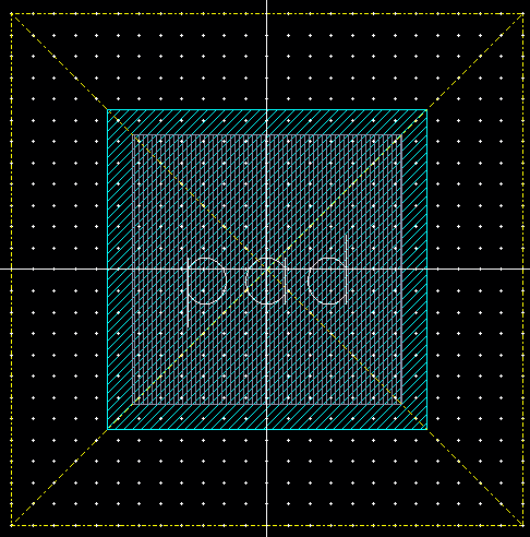
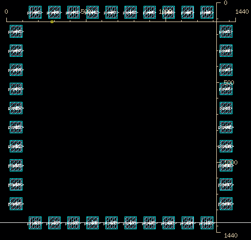
Now we need to number each pin individualy. Remove the pad layer on the pad layout.
This will help speed up selection. Follow the numbering scheme in the
tutorial. You should have something similar to the layout below.
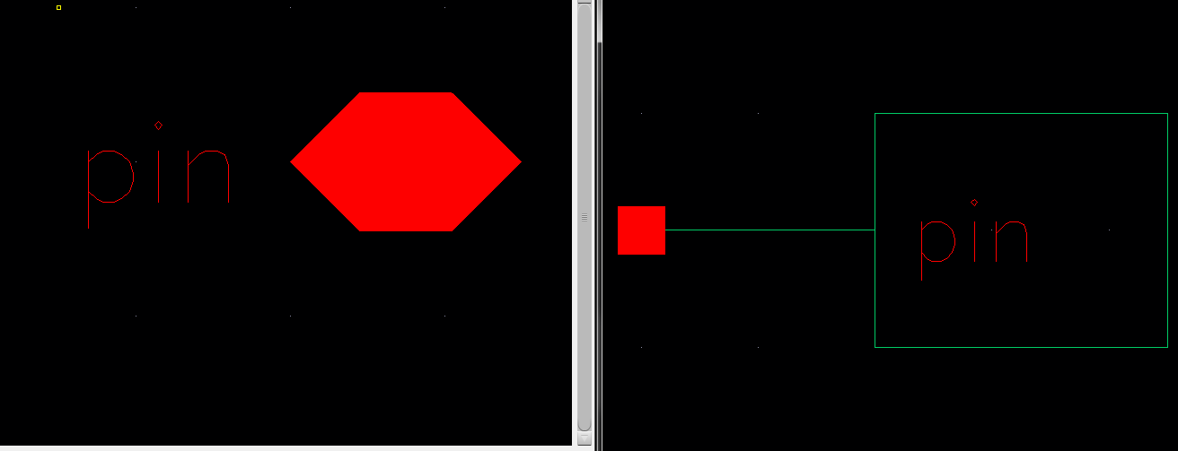
Now create symbol and schematic for the pad. For the schematic simply place an inputoutput pin called pad. Create the symbol and simplyfy as below.
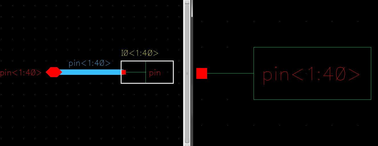
Now do the same for the pad frame. As always DRC and LVS.
I later added metal1, metal2, via, and via2 so that my pads can connect with any metal layer.
The
rest of the tutorial involves adding additional items and connecting
them to the frame. We are going to skip that part becuase we will not be using that information in lab 7.
___________________________________________________________________________________________
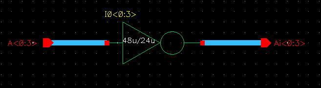
Lets
begin with the 4bit inverter. Create a new schematic for the 4 bit
inverter and instansiate a 1 bit inverter. Place input and output pins.
Make sure that you use arrays for the pins and thick wires to connect
them. You should have a shematic similar to the one below.
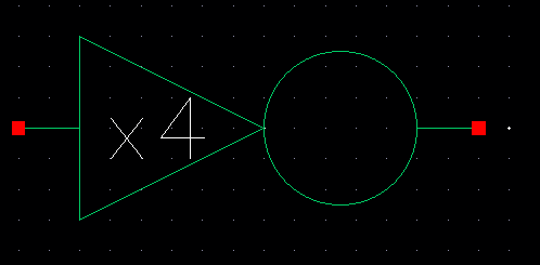
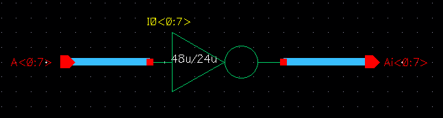
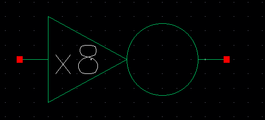
Next create a symbol. Make sure that you differentiate it in some way from the 1 bit inverter. I use x4 to denote 4 bits.
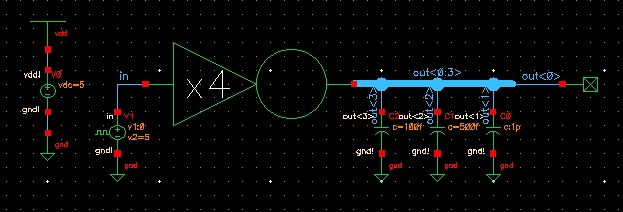
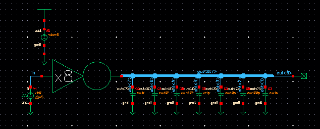
Now
that we have a symbol and a schematic we will simulate the inverter.
Per lab requirements will be attaching capacitors on to 3 of the
outputs and oberserving the effects of the capacitors on the inverter.
I chose to pulse my input at 5nS pulses and a 10nS period. Have the
schematic laid out similar to the image below.
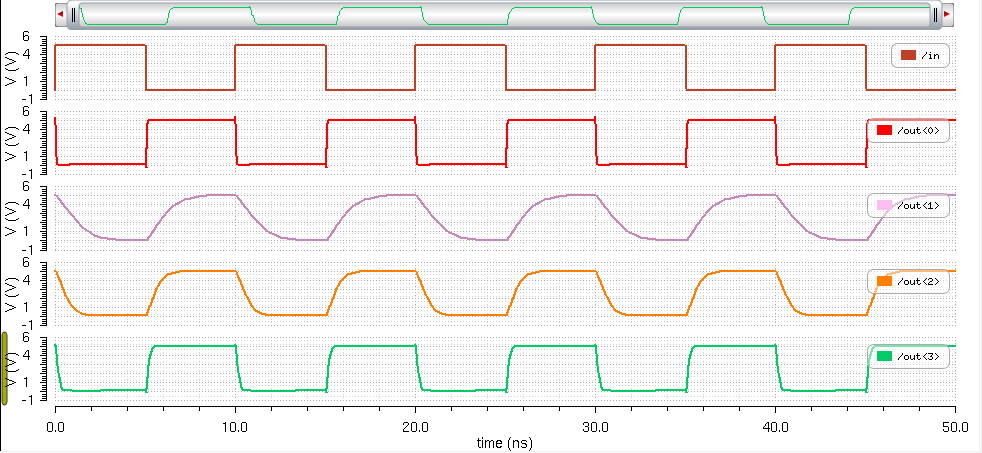
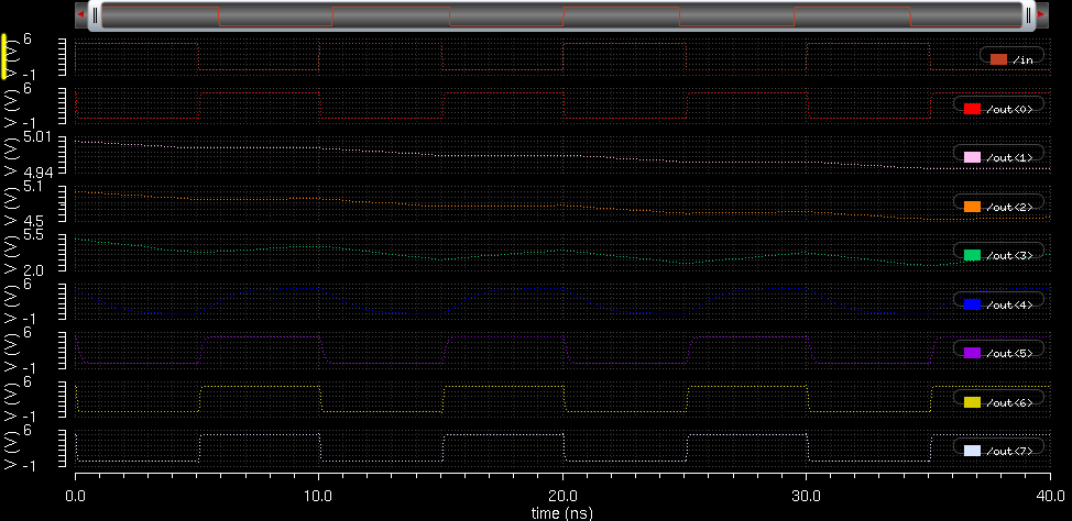
Next
launch ADE-L and run a transient analysis. Plot all the outputs and the
input. Set the run time for 50nS. You should see how the increased
capacitances reduce the retangular shape of the input intu a more
curved wave.
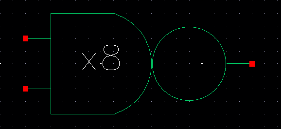
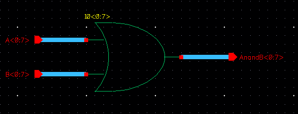
Next we will go to the 8 bit nand gate. As before create a schematic and symbol.
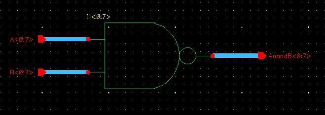
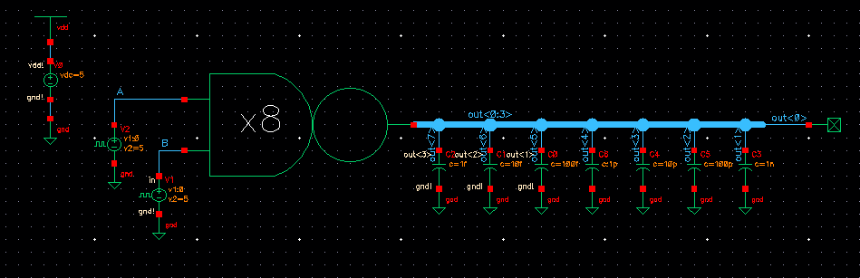
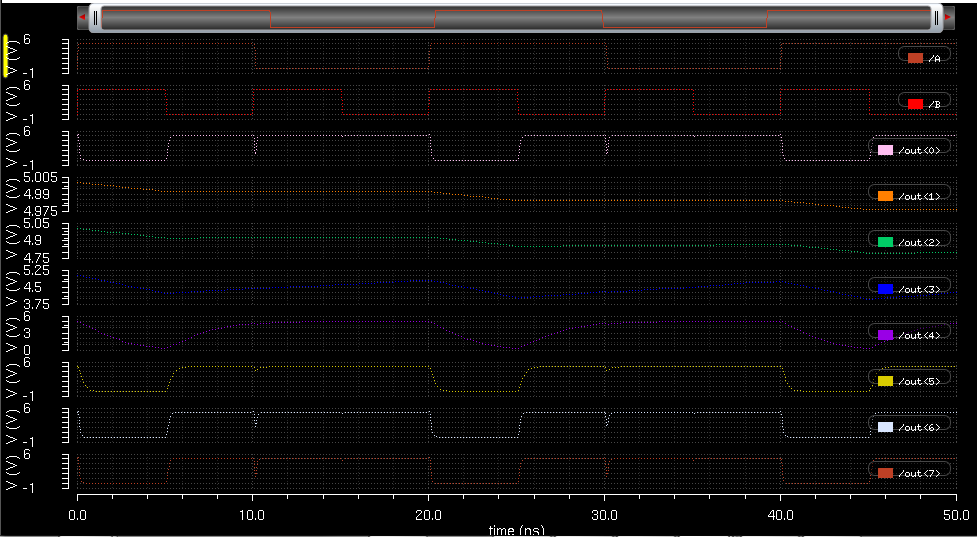
Now
simulate the 8 bit nand gate in a circuit. Again you should notice the
deviation of the square wave form with higher capacitances. I started
at 1fF and increased capacitances by 1 order of magnitude at a time.
Since the lab requires an 8 bit inverter i will repeat the process.
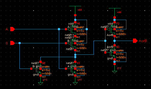
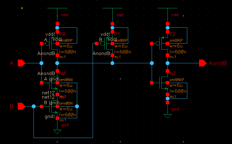
The lab requires nor, or, and and
gates. We haven't created these previously. I am going to create the
nor gate. I'll start with the 1 bit nor gate. The schematic is as
below. Please refer to page 353 of the text book for more
information.
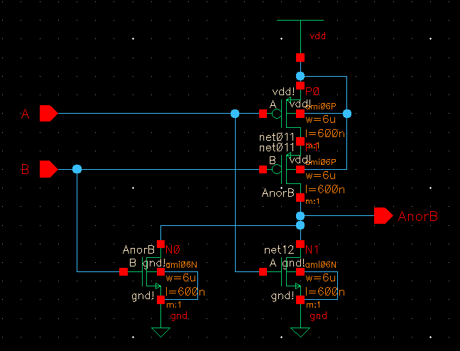
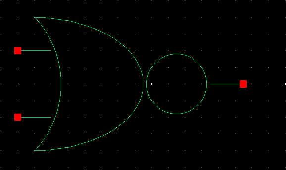
Then create the symbol.
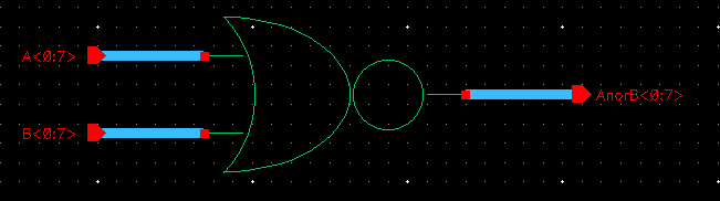
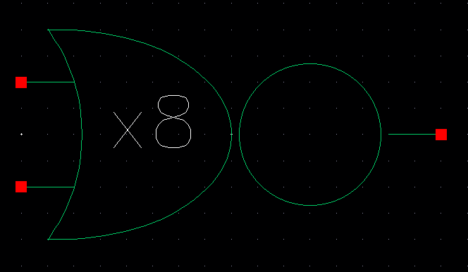
Then we create the 8 bit nor schematic and symbol.
From the nor schematic it is a simple process to create an or gate. My solution was to add an inverter inplace of the regular output.
Please check that all the nmos and pmos used are 6u/0.6u.
After creating the schematic create the symbol as below.
Then repeat the earlier process to create the 8bit or gate.
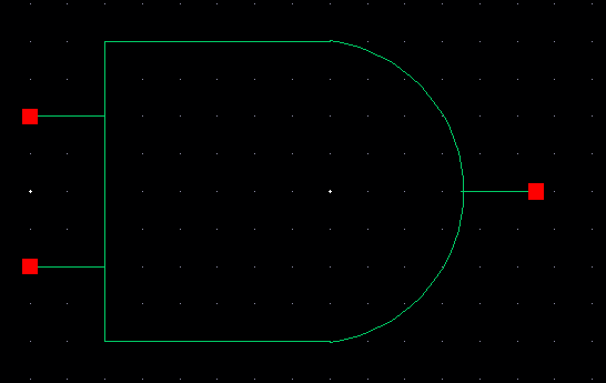
I followed a similar procedure for the and gate. Take the nand schemtaic and add an inverter.
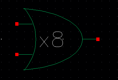
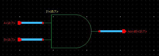
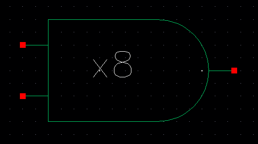
Then repeat the earlier process to create the 8bit and gate.
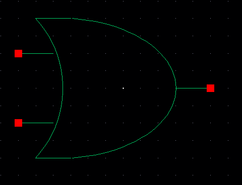
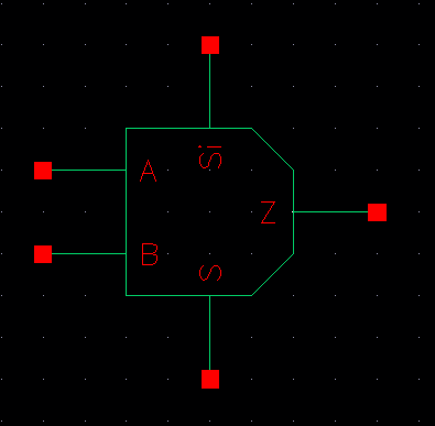
The final component needed is the 2-1 mux. Below is the schemtic and symbol for the mux.
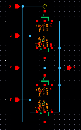
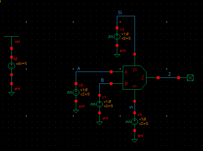
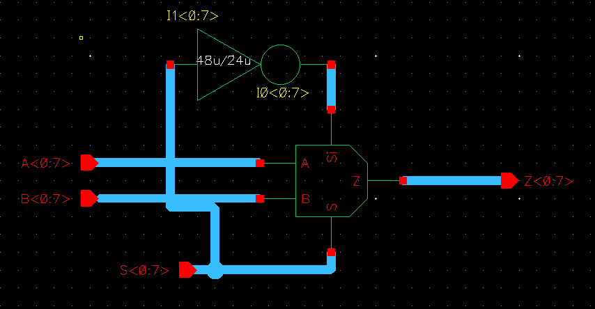
Then
we need to simulate the mux. Lay out the schematic as below. One of the
inputs needs to go at twice the speed of the other. Make sure that S
and Si are opposite. I did this by reversing volatge 1 and voltage 2
for one of the pulse sources. One of the of the pulse sources goes
from 0 to 5V the other goes from 5V to 0.
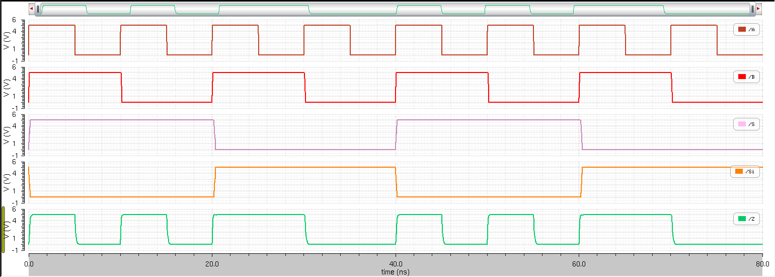
Look at
the output of the simulation. Notice that when S is 1 and Si is 0 the
output is A. When Si is 1 and S is 0 the output is B. The mux chooses
between A and B depending on S.
For a de-mux the
input and output pins need to be changed around. What would happen is
that the S would select if the signal from Z went to A or to B. As the
mux is it can not be used for a de-mux.
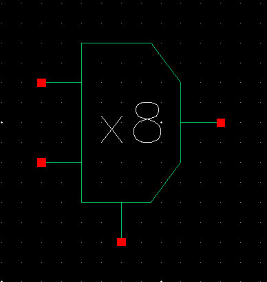
It should be obvious by now that the next step is an 8 bit mux. Use an inverter so that you will not have S and Si input pins.
And then create the symbol. I have reomved the labels for the pins to reduce the clutter.
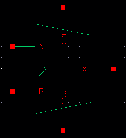
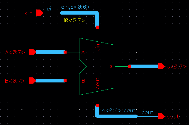
The
last piece required for this lab is the full adder. This is a different
design from the previous full adder. Follow the schematic below or
refer to figure 12.20 in the text book. To prevent a mixup with the adder from the earlier labs I have added 12 in to the name of the cell view.
I used the inverter from
NCSU_Digital_Parts and chaged the W for the nmos and pmos to 6um. I
left the inputs as upper case A and B to differenciate from the
previous design.
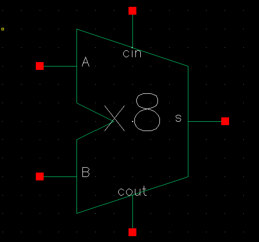
The symbol is similar to the one created earlier.
The
lab requires a layout of the 8 bit adder. To make things slightly
easier lets begin with the 1 bit layout. I kept metal 1 and metal 3 for
the vertical connections and metal 2 for the horizontal connetions.
This makes it easier to keep track of the connections in my opinion.
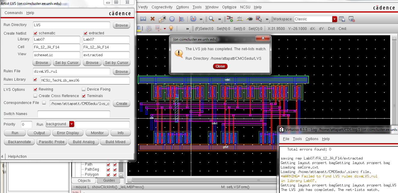
DRC and LVS the layout to fix any issues at the 1bit stage.
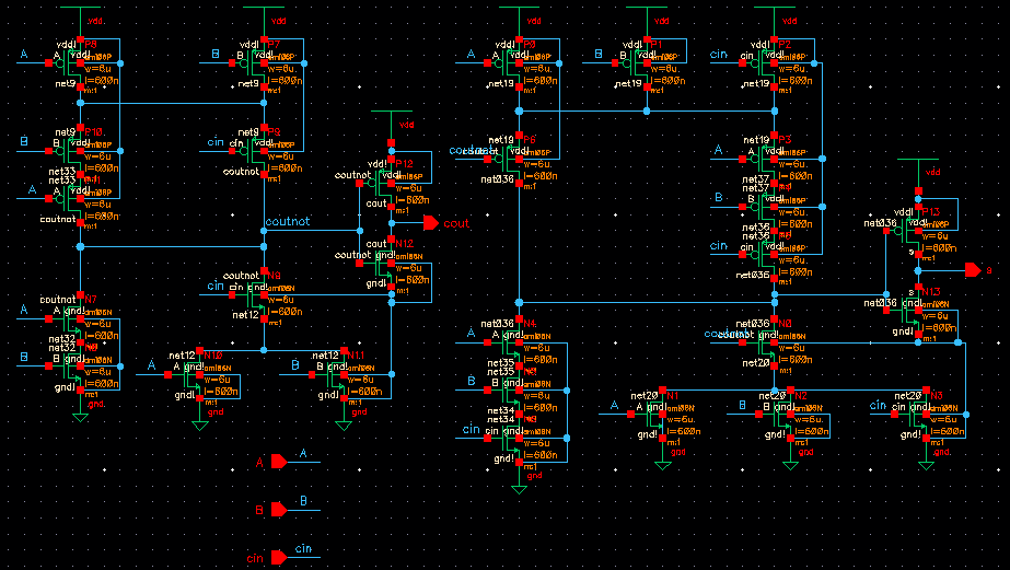
For
the final part of the lab we will be creating the 8 bit adder. Begin
with the schematic. Use thick wire and arrays as done in the oscillator
to connect the carry-ins and the carry-outs.
Create the symbol as the 1bit adder and add the x8.
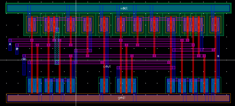
Now lets create the layout. You will have to set them next to one another and connect each carry to the next. All the vdd! s and gnd! s need to be turned into one pin. You will have a long or tall layout depending one the orentation you use. Finally add the cin, cout,
and the other input output pins. remember to add the A, B, and S pins
as a part of an array. Below are the 0th, 1st, and 7th bits of the
adder.
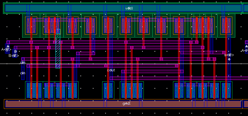
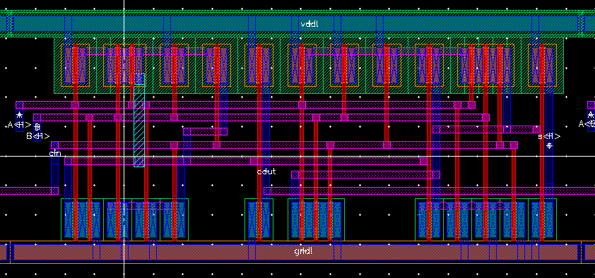
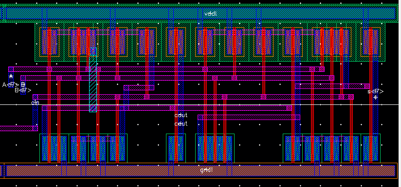
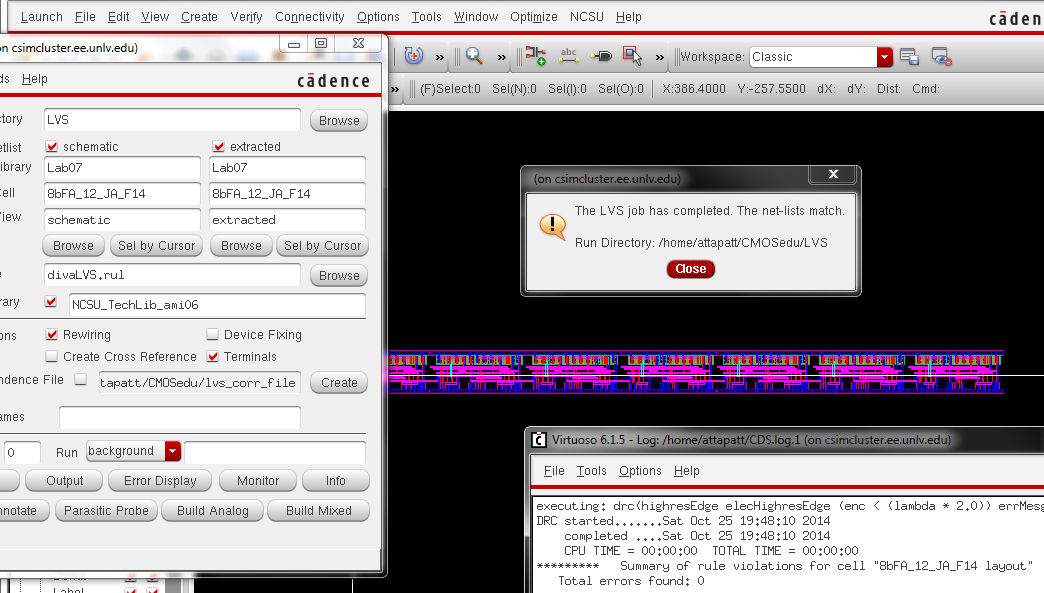
DRC and LVS your adder.
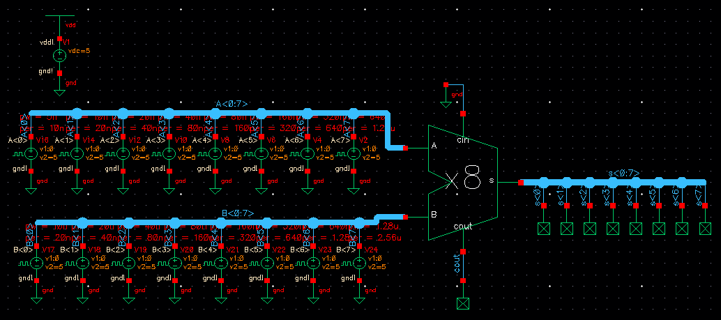
The
final requirement for this lab is the simulation of the 8 bit adder.
This is a slight problem. A has 2^8 possible values, B has 2^8 possible
values and cin has another two possible values. This gives a total of
2^20 possible inputs. So just create a few inputs of your own choice
and check if they are as expected. I chose to set my cin to ground. I set the pulse sources to different pulse widths and periods.
Now launch ADE-L and plot the inputs vs the outputs. As you can see it is not very distinguishable.
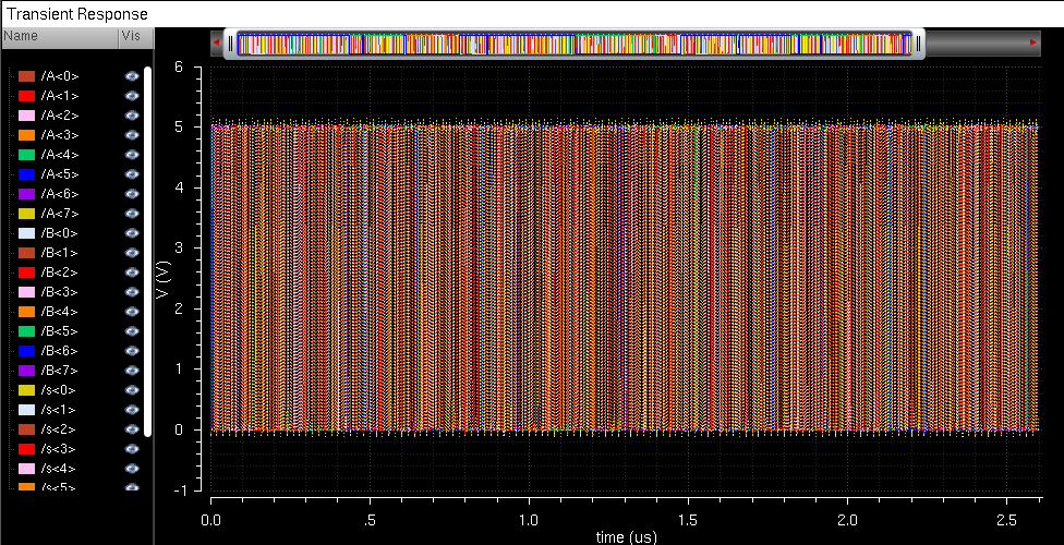
Split by trace and view one segment at a time to check as you want.
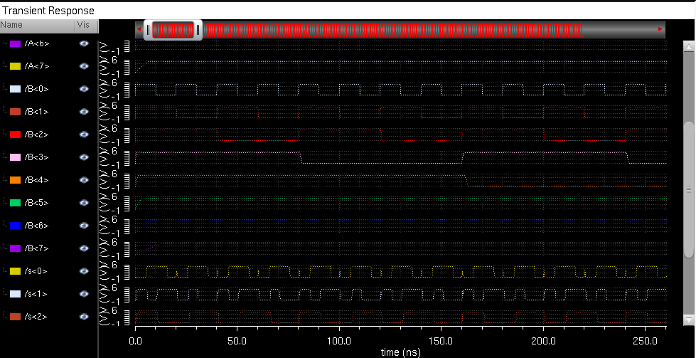
This is still not very easy to read but it is readble if you want to check.
As in the last lab I have appended _JA_F14 to the cell names.
Backup your work.

That concludes the end of this lab. Here is the design directory used in this lab.
Return to EE 421L Labs