Lab 06 - ECE 421L
Authored
by Jeevake Attapattu,
attapatt@unlv.nevada.edu
10/13/2014
Simulation and layout of a Full Adder using NAND and XOR gates
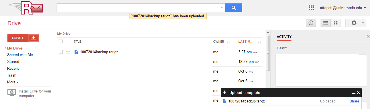
Using MobaXTerm log into csimcluster.ee.unlv.edu. The first action is creating a backup. Type tar -cvf "date"CMOSedu.tar CMOSedu/. This will create a tar file
with all the project and homework saved. In place of "date" type in the
date creating the backup. Unce the backup has been created type gzip "date"CMOSedu.tar.tar. This will create a .tar.gz file witch is significantly smaller.
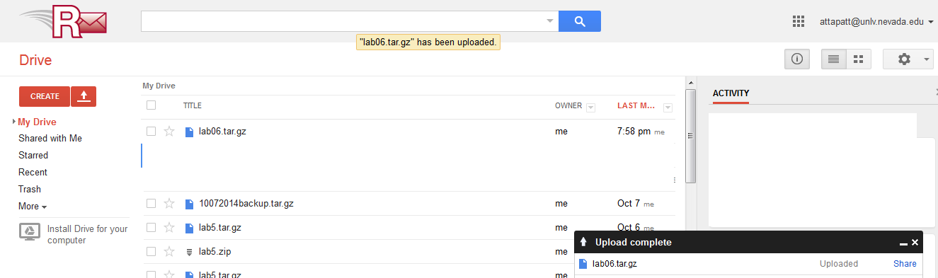
Use MobaXTerm to download the file to your own pc then upload to a backup site such as dropbox or google drive.
Launch Virtuoso.
You will be using previous work from tutorial 4.
Download all tutorials if needed from here.
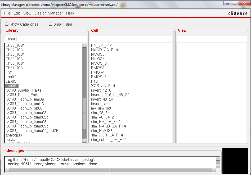
In the library manager copy the files in lab 5 to lab 6.
Make sure that you update intances when copying.
Open
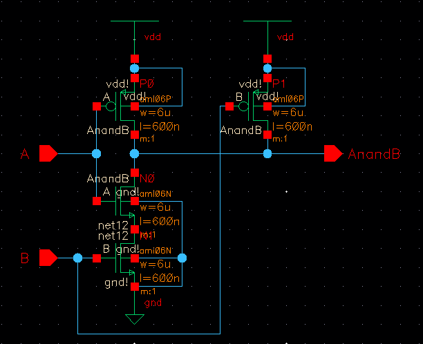
a new schematic called not since we are going to create a NAND gate. We
will be using the inverter used created in lab 5. Layout as
seen in the schematic below. Change the pmos to a 6u/0.6u
pmos and make sure that the nmos is the same. Copy the nmos and pmos
for extra instances and wire as below. Change the output to AnandB and add an extra input B.
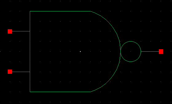
Delete the previous symbol that was copied over. Then go to create->cellview->from cellview. You will need to create the NAND symbol as seen below. Use the classical NAND symbol.
Open the layout cellview to for the layout of the inverter. Use a large
vdd! and gnd!, it will be a good habbit. Copy the nmos and pmos and over lay with the previous ones.
We
must get rid of the pins in the middle of the nmos. Select the first
nmos the hold shift as you select the second nmos. Go to edit->hierarchy->flatten. Unselect preserve pins geometries. Select flatten pcells, and flatten vias. Delete the vias and metal 1 in the middle.
Change the pmos width to 6u per lab requirements. Add the AnandB pin. Remeber that it is an ouput.
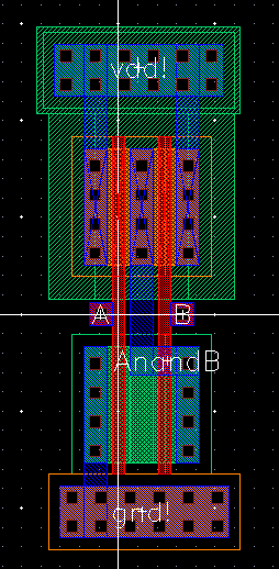
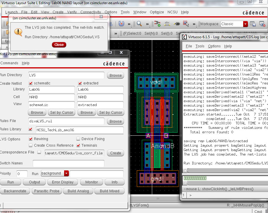
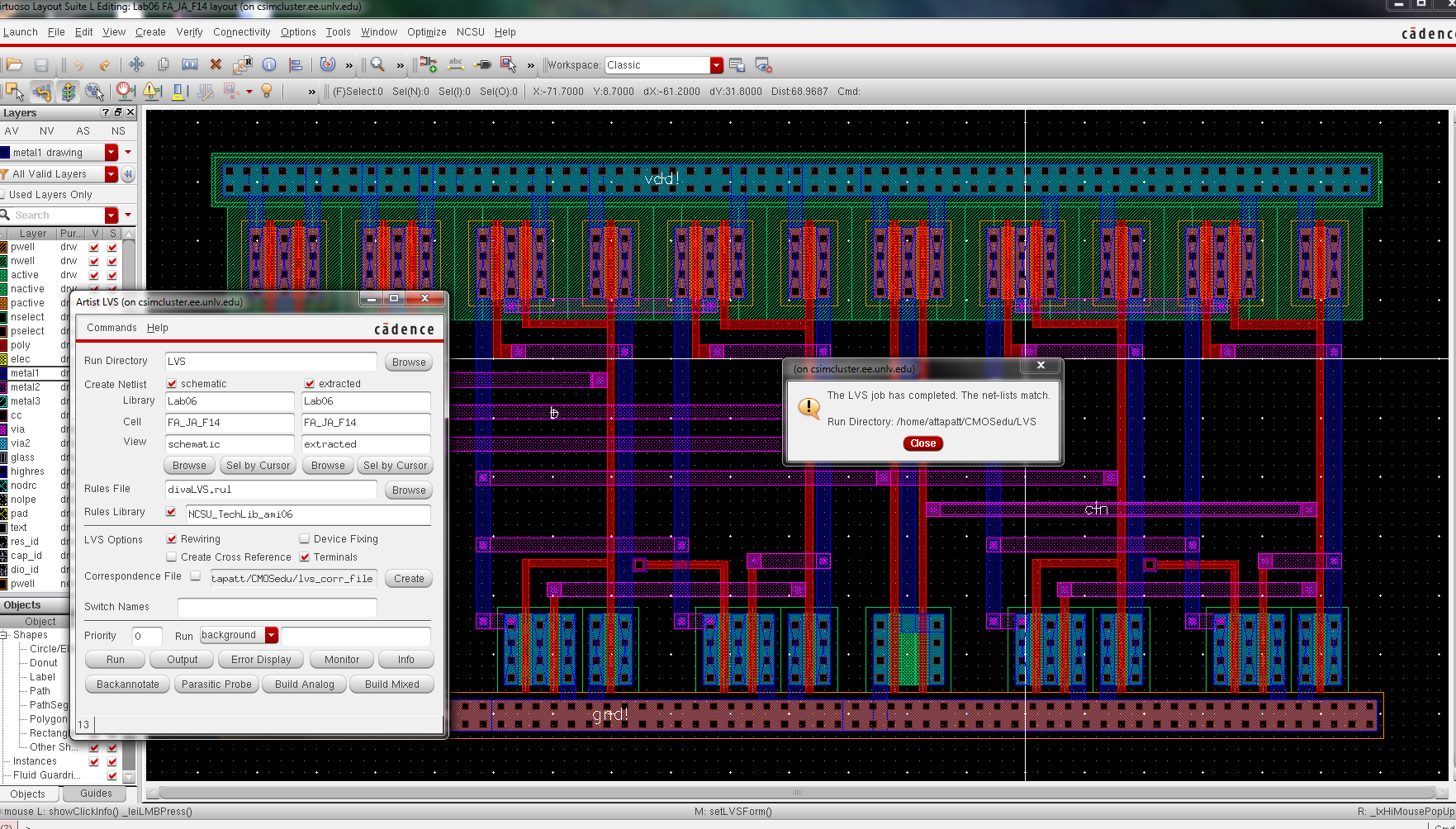
DRC for design errors then extract and LVS. You should have something similar to the image below.
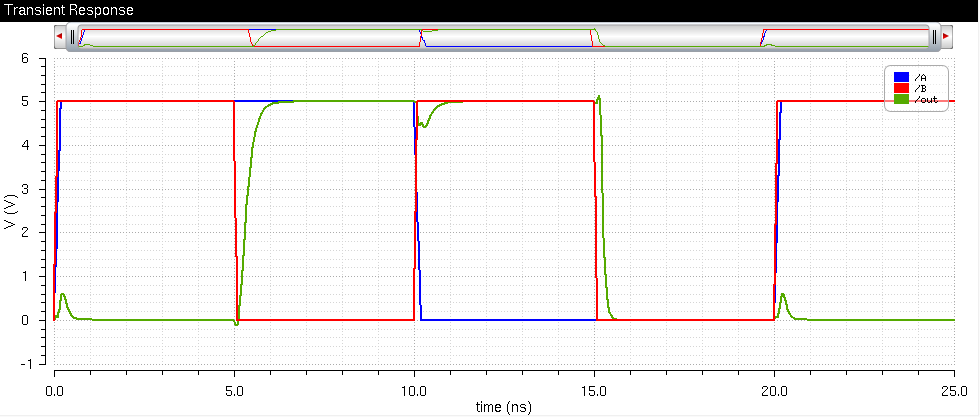
Now
lets simulate the NAND gate. Create a new cell view schematic for the
simulation. Use two pulse inputs. Set one with twice the period of the
other. I have chosen 5nS and 10nS periods.
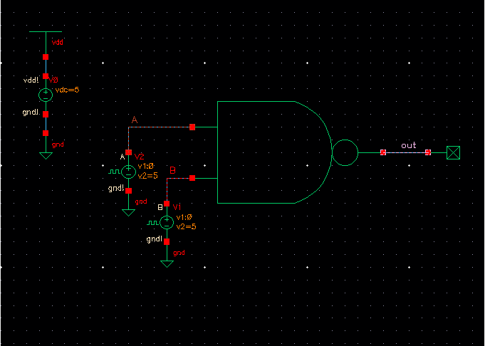
Launch ADE-L
and do a transient analysis for the time you are looking at. I have
chosen 25nS. Plot the inputs against the output.
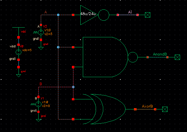
Next we repeat the process for the XOR gate.
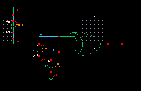
First create the schematic. It is more complicated so make sure that it follows the image below.
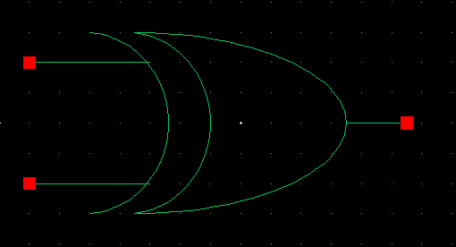
After creating the schematic, create the symbol. Use the classical symbol for the XOR gate.
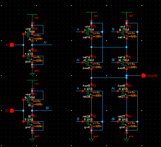
The
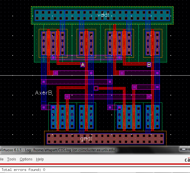
next step is to create the layout. Again the layout is more complicated
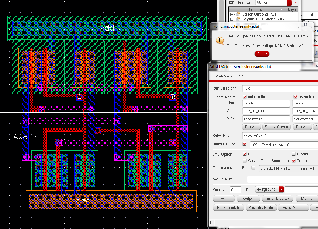
so make sure that your layout is similar to the one below. Afterwards DRC and LVS.
Now test the XOR gate in a simulation similar to the one used for the NAND gate. Use ADE-L to do a transient analysis.
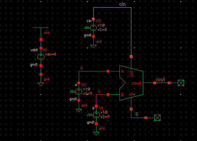
Now that we have working NAND and XOR gates we can build a full adder (FA). The FA is designed similar to the schematic below.
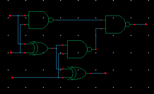
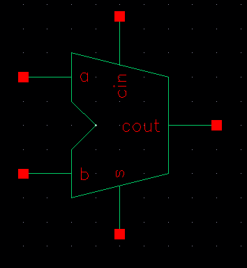
Use the classis design of a FA for the symbol.
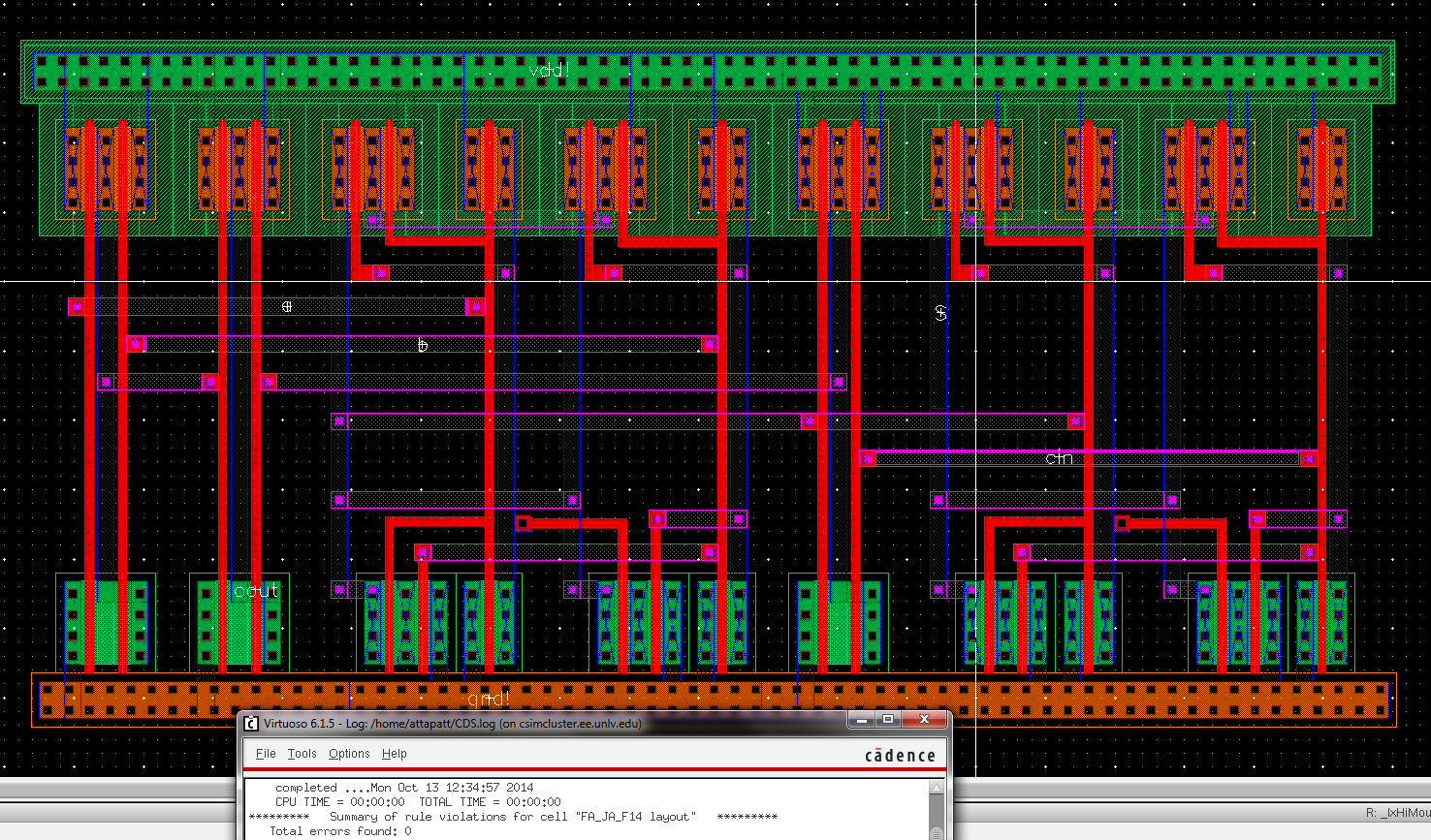
Now
we have to do the layout. Pay carful attention to the image below. The
FA layout is very complicated. I used metal 2 for horizontal
connections and a few of the pins. I copied and pasted the layouts from
the NAND and XOR gates. When you do this remove the extra vdd! and
gnd!. Leave one of each and expand the number of columns.
I placed
metal 1 to poly and metal 1 to metal 2 vias on top of one another where
metal 2 connects with poly. it reduces clutter. Be carefull about your
output/input selection of pins when you place them. DRC and LVS the
layout.
For
the final step of the FA we must simulate the FA with 3 pulse sources.
I used 10nS, 20nS, and 40nS periods with a transient time of 90nS.
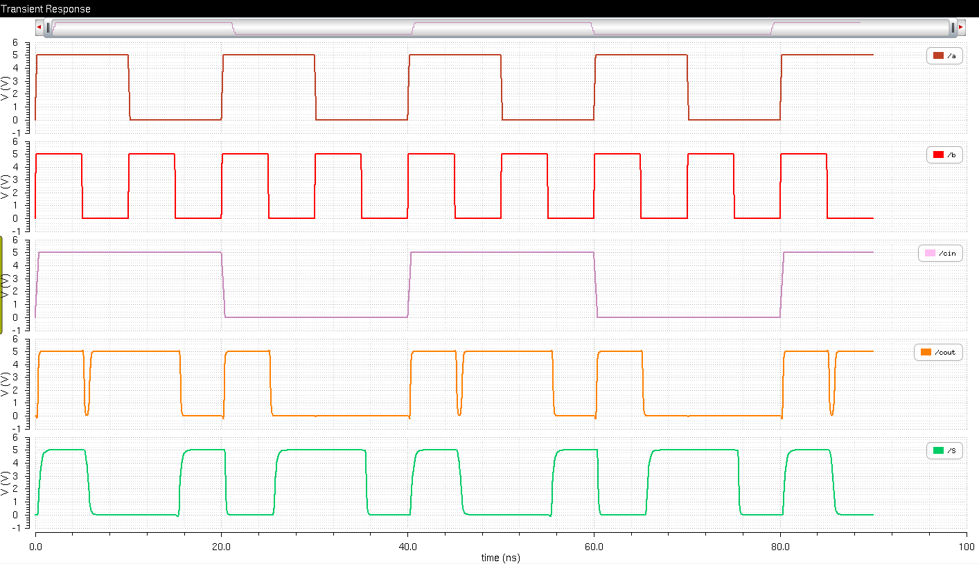
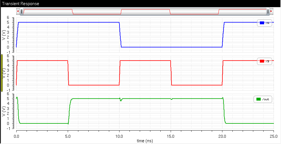
Finally, as per lab requirements we have to simulate the schematic as below.
You
should have a ADE-L plot similar to the one below. If the traces are
together, right click on the graph and select split trace.
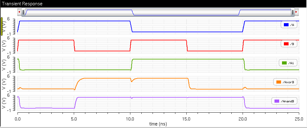
You
should notice in the image above and all the rest of the plots in this
lab that the outputs are not perfectly square pulses. There are delays
for the gates to perform each logic operation. These delays are clearly
visible on the nano second scale I have used.
Zip your lab directory and backup. I uploaded mine to google drive.
Here are my cells for this lab. The ones I specifically created and used in this lab have JA_F14 appended to the cell names.
That concludes the end of this lab. Here is the design directory used in this lab.
Return to EE 421L Labs