Lab 05 - ECE 421L
Authored
by Jeevake Attapattu,
attapatt@unlv.nevada.edu
10/06/2014
Simulation of inverters using NMOS and PMOS
Using MobaXTerm log into csimcluster.ee.unlv.edu. The first action is creating a backup. Type tar -cvf "date"CMOSedu.tar CMOSedu/. This will create a tar file
with all the project and homework saved. In place of "date" type in the
date creating the backup. Unce the backup has been created type gzip "date"CMOSedu.tar.tar. This will create a .tar.gz file witch is significantly smaller.
Use MobaXTerm to download the file to your own pc then upload to a backup site such as dropbox or google drive.

Launch Virtuoso.
You will be using previous work from tutorial 3.
Download all tutorials if needed from here.
In the library manager copy the files in lab 4 to lab 5.
Make sure that you update intances when copying.
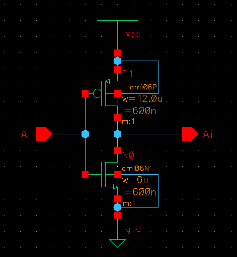
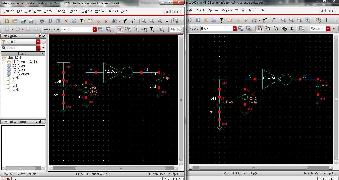
Open
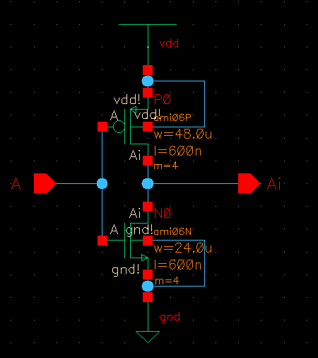
a new schematic called not since we are going to create an inverter. We
will be using the 4 pin PMOS and NMOS used created in lab 4. Layout as
seen in the schematic below. Label the top node as vdd!. We will supply a value for vdd later. Name the input pin A and the output pin as Ai for A inverted.
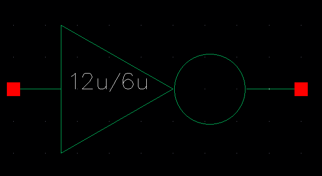
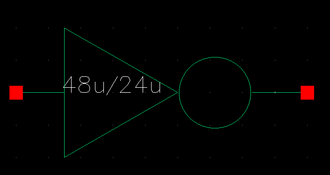
Go to create->cellview->from cellview. You will need to create the inverter symbol as seen below. Include the label to indicate the with of the mosfets used.
Open
a new layout cellview to for the layout of the inverter. Use a large
vdd! and gnd!, it will be a good habbit. Get the nmos and pmos from NCSU_TechLib_ami06. Rember to use 12u for the pmos and 6u for the nmos.
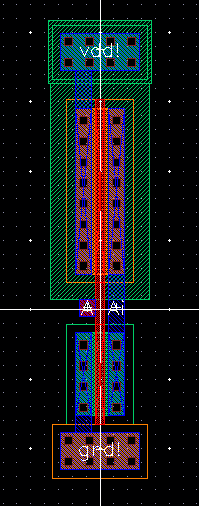
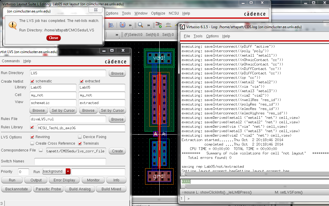
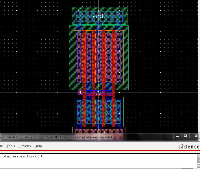
DRC for design errors then extract and LVS. You should have something similar to the image below.
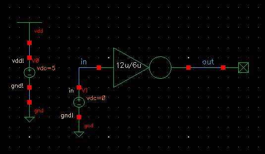
Now
that the inverter has been created we can simulate it. Create a new
cellview schematic. Add the inverter and a voltage for input. Set the
voltage to 0. To meassure to uoput without an error use a noConn.
instanciate, go to baasic->Misc->noConn. This is where we will define vdd!. Add a second voltage source at 5V.
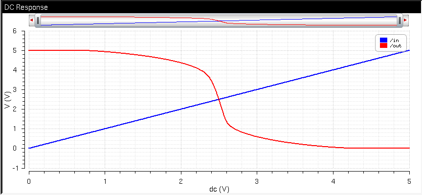
Launch ADE-L. We will now simulate the inverter. Choose dc analysis with component parameter. Set the rest as below.
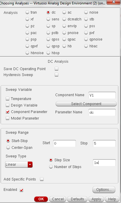
Choose in and out from the schematic to be plotted. Add the model libraries as done previosly in lab 4. Run the simulation.
End of Prelab
________________________________________________________________________
Now
we will repeat the process for a 48u/24u inverter. Copy the last
inverter schematic into a new cellview. Type q on each mosfet to edit
the properties. Change the pmos W to 48 and the nmos to 24. Change the
multipliers on each to 4.
Copy the symbol created for the previous inverter and edit it.
Now
we create the layout. Open a new layout. Go to the properties of each
mosfet and change the the multipliers. Attach everything as
below and DRC.
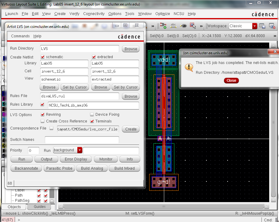
Extract and LVS.
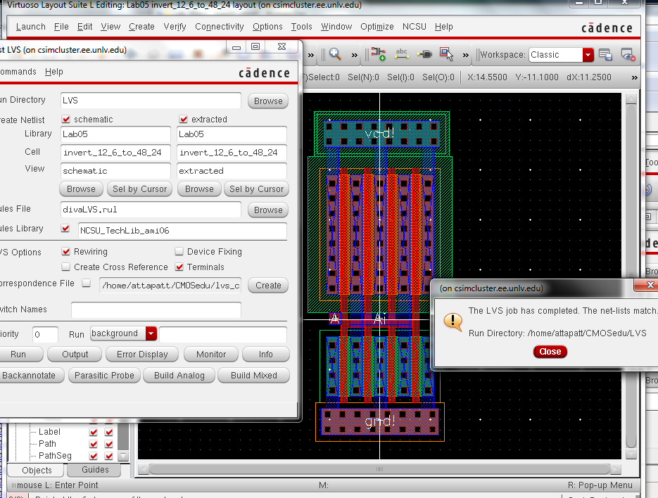
And as per lab requirements the lvs of the 12u/6u.
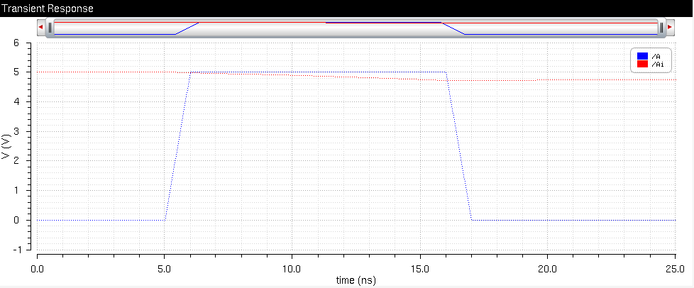
Now
we must run simulations of the inverters driving capacitors with a
pulse input. Lets begin with the 100fF load for the 12u/6u
inverter. Check and save the scematic each time before running the
simulation in ADE-L.
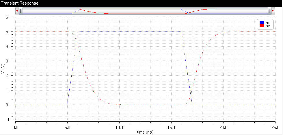
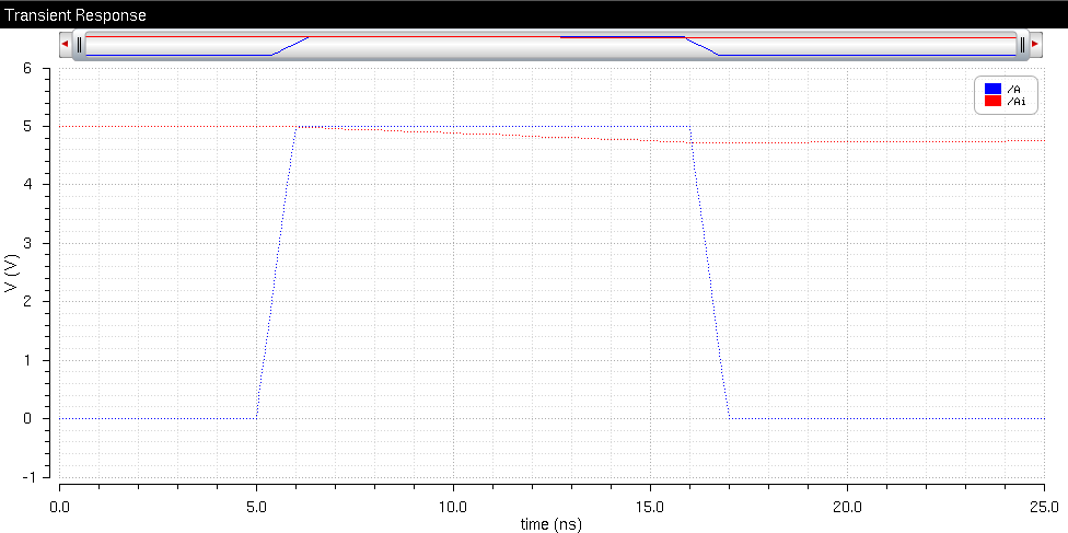
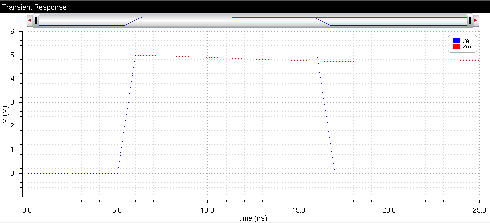
The 100fF load.
12u/6u
inverter.
48u/24u inverter.
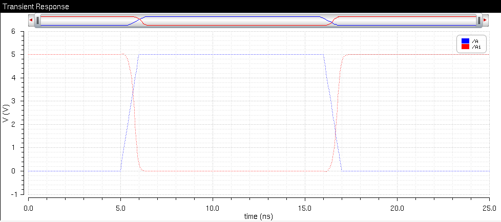
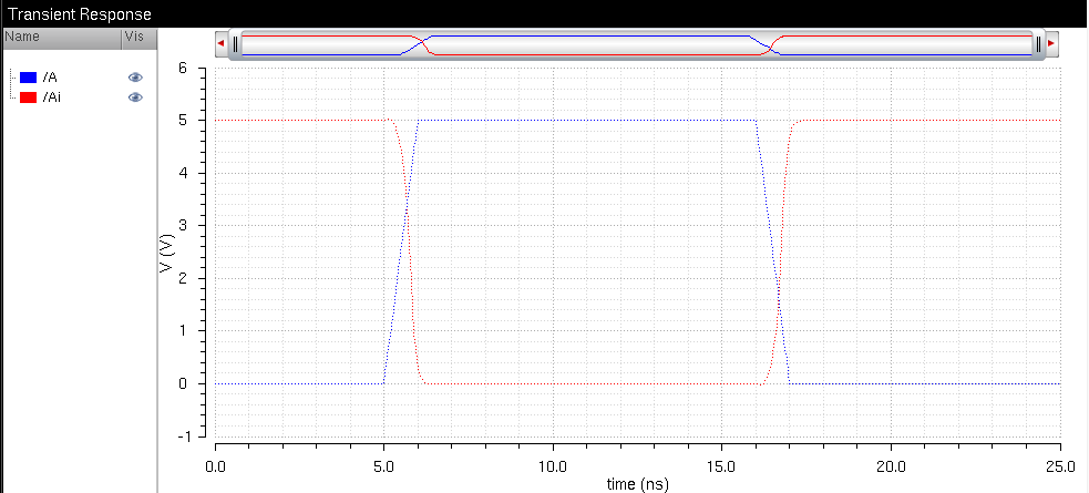
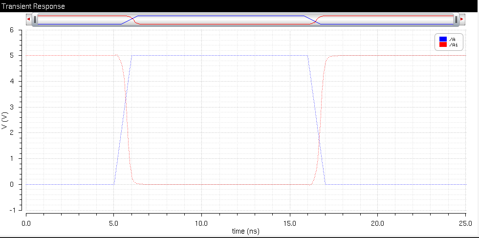
The 1pF load.
12u/6u
inverter.
48u/24u inverter.
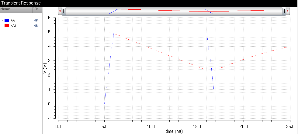
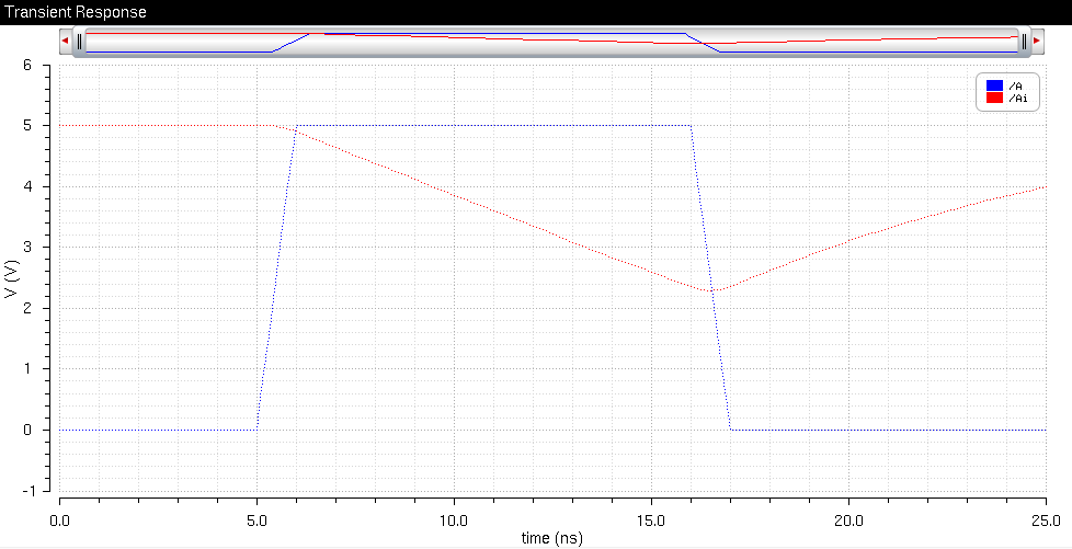
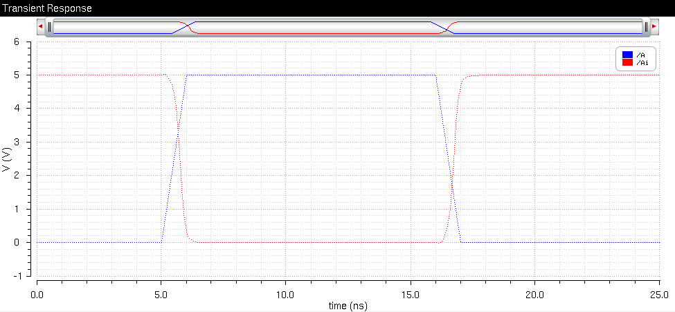
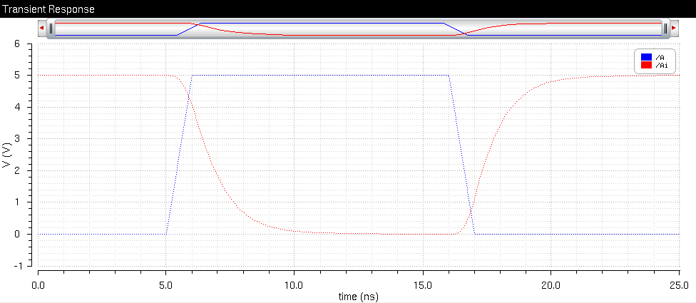
The 10pF load.
12u/6u
inverter.
48u/24u inverter.
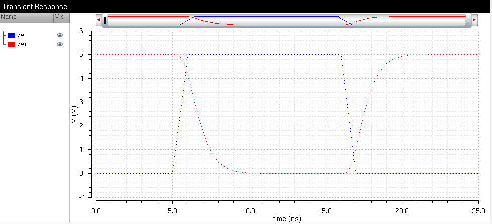
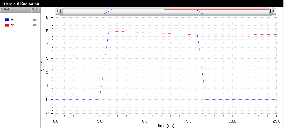
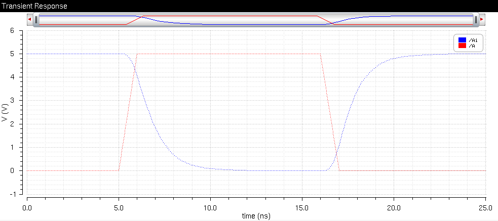
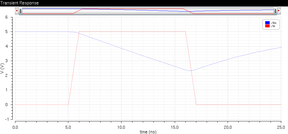
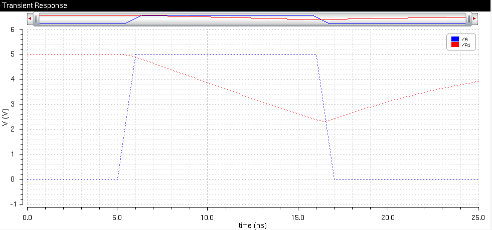
The 100pF load.
12u/6u
inverter.
48u/24u inverter.
As
the capacitance is increased it takes longer for the voltage output to
change. And the 48u/24u inverter responds slighty, though insificantly better than the 12u/6u
inverter for larger capacitors.
Now we will repeat the last few simulations using UltraSim instead of Spectre. Launch ADE-L and go to setup->simulator/directory/host and select UltraSim from the drop down menu instead of Spectre. Remeber to include the stand alone model libraries.
The 100fF load.
12u/6u
inverter.
48u/24u inverter.
The 1pF load.
12u/6u
inverter.
48u/24u inverter.
The 10pF load.
12u/6u
inverter.
48u/24u inverter.
The 100pF load.
12u/6u
inverter.
48u/24u inverter.
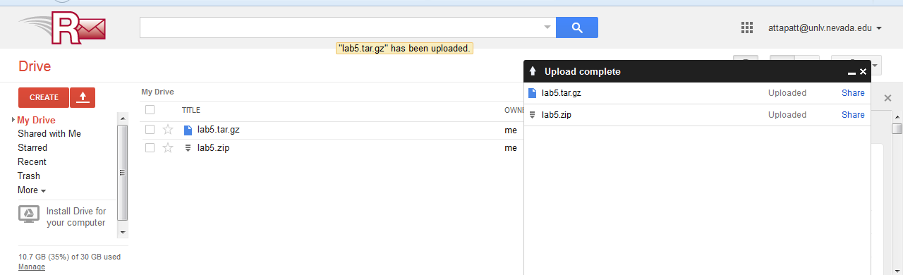
Once
finished backup design library and the directory where the lab report
was created. The tar file is the design library and the zip file is the
lab report directory.
That concludes the end of this lab. Here is the design directory used in this lab.
Return to EE 421L Labs