Make sure to go over Tutorial 5 and Electric video 11 here
Learning to use buses and arrays:
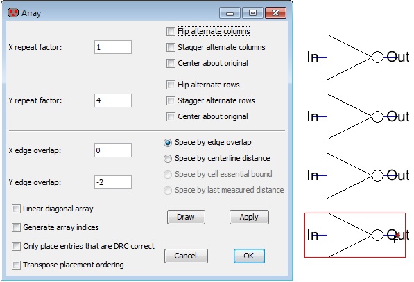
1) open a new cell schematic and name it inverter_array and copy the inverter. Click on Edit->Array (or press F6) to use the array command.
2) change the y repeat value to 4 and the y-edge overlap to 2
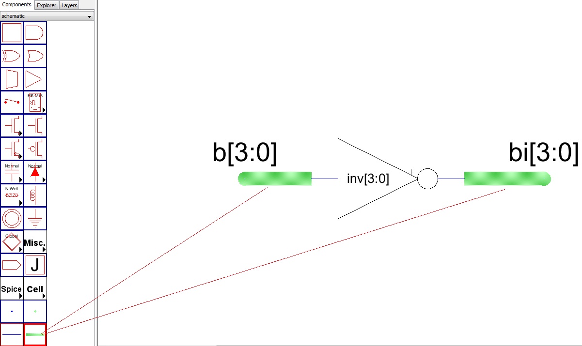
3) open a new cell schematic and name it inverter_bus and copy another inverter in it
4) ctrl+i and change the name to inv[3:0] meaning you have 4 inverters from inv[0]->inv[3]
5) go to the component tab and click the bus symbol which is the bottom right green wire
6) create the input and output exports using the bus as seen below and export them
Creating a ring oscillator:
1) open a new schematic and call it ring_oscillator
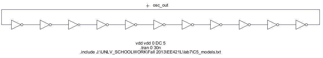
2) copy an inverter into the schematic and copy it to obtain 11 inverters by using the array command F6 x-repeat: 11, x-overlap: -5
3) connect the inverters together and set the last inverter's output to be the first inverters input
4) label the last wire's arc as osc_out
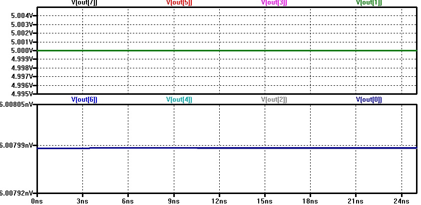
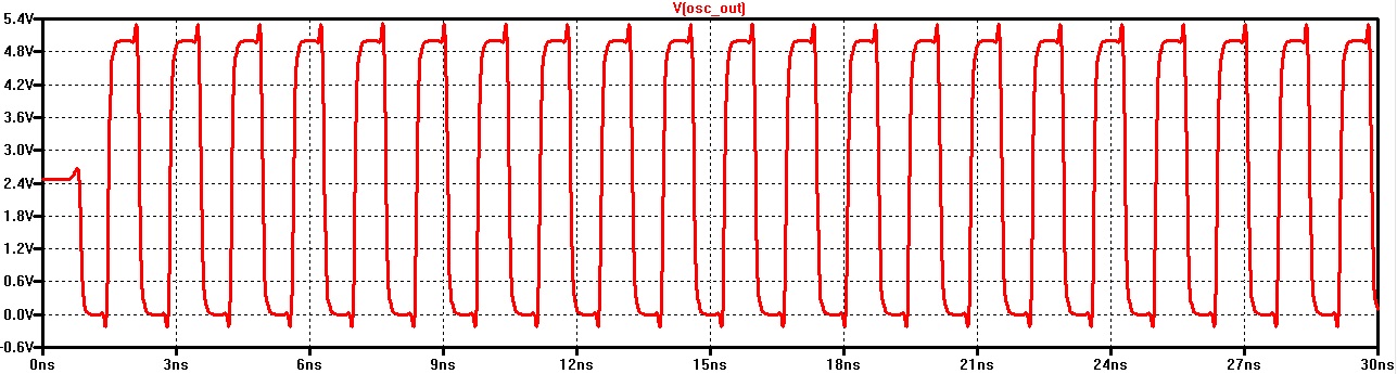
5) add spice code seen below, schematic should look as follows
6) simluate the schematic to obtain the following results
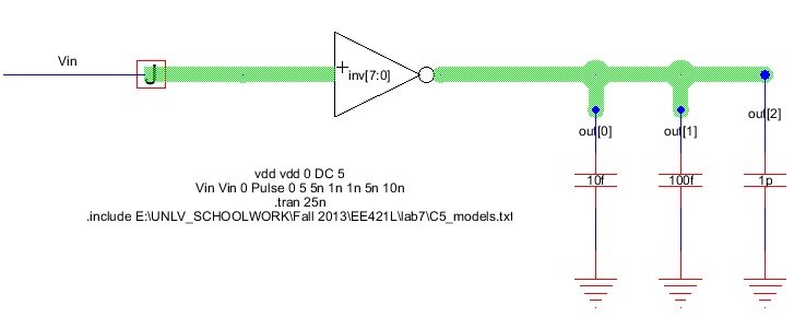
Create an 8bit inverter

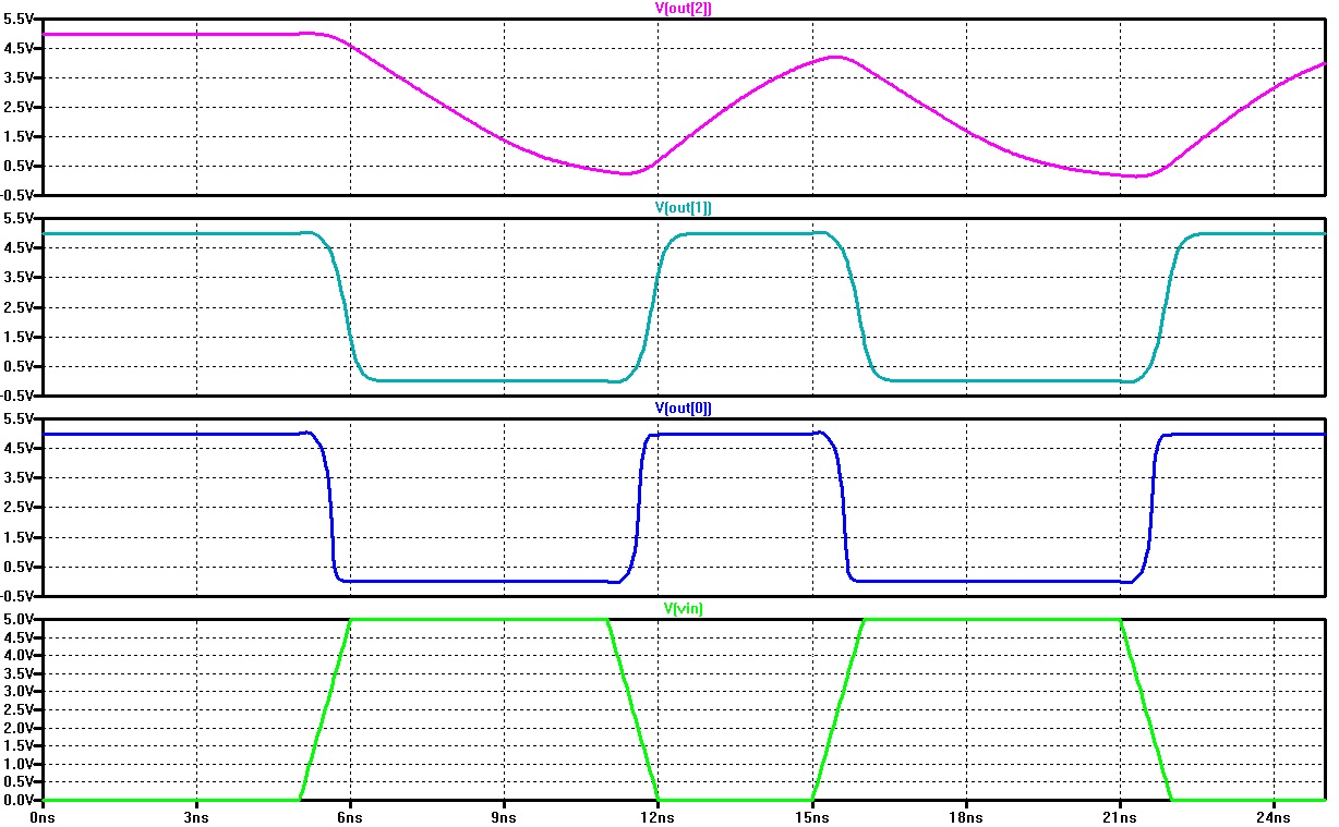
Simulate the inverter with different capacitive loads
Simulation results
NAND
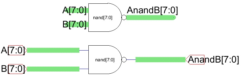
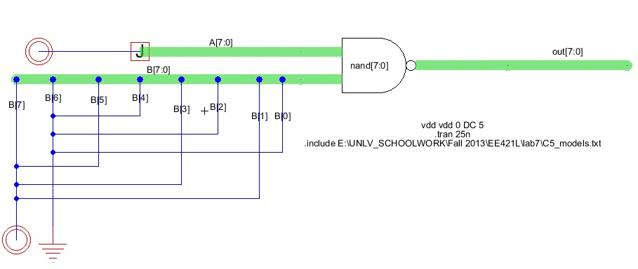
the following schematic shows the nand operation of A=11111111 and B=10101010
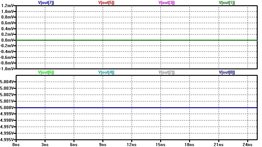
the following simulation shows the nand operation of A=11111111, B=10101010 which results to AnandB=01010101
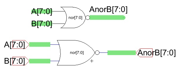
NOR
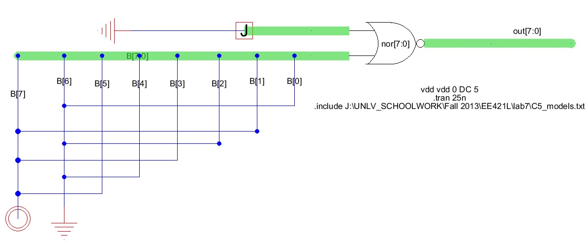
the following schematic shows the NOR operation of A=00000000 and B=10101010
the following simulation shows the results of the NOR operation of A=00000000 and B=10101010, AnorB=01010101
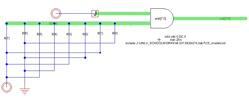
AND
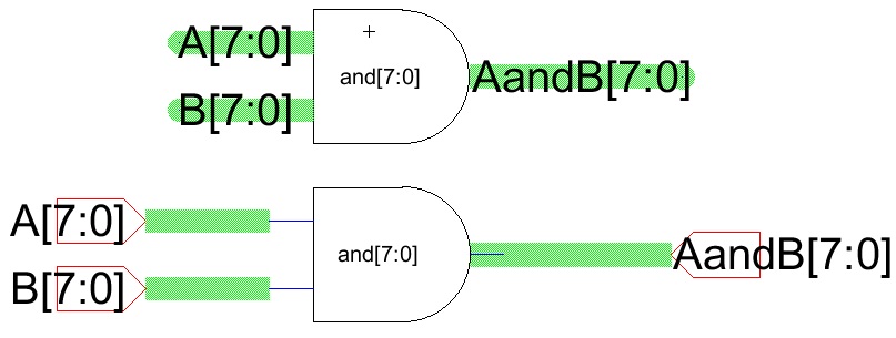
the following schematic shows the AND operation of A=11111111 and B=10101010
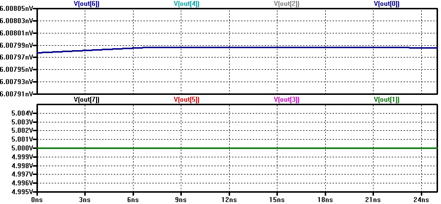
the following simulation show the AND operation resulting in 10101010
OR
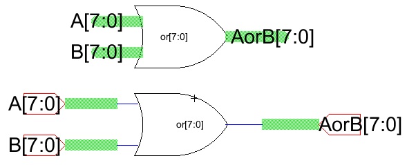
the following schematic shows the operation of A=00000000 and B=10101010
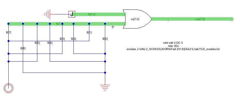
the following simulation shows the results of AandB=10101010