- show layout
Make sure to go over Tutorial 4 and Electric video 11 here
NAND gate:
Schematic:
1) duplicate the cell inv_20_10 cell and name it NAND_gate
2) change MOSFET sizes to width=10 and length=2
3) delete all the wires leaving just the MOSFETS in the drawing area
4) copy and paste each MOSFET resulting into 2 total NMOS/PMOS devices
5) copy and paste the power source
6) place a label and export it naming it AnandB, also rename In->A and Out->B
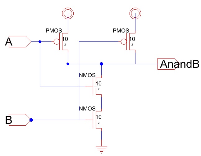
7) place the components in the schematic and connect them with wires as seen below
Icon View:
1) go to the Explorer tab, look for NAND_gate{ic} and open up the cell
2) using the circle and polygon component, draw the icon for a NAND_gate, use the Tool Outline Edit
3) with the polygon tool, draw a square with one side missing (right side)
4) with the circle tool, press ctrl+i and change the degrees to 180, connect it to the missing side of the polygon
Simulation:
1) First do a DRC (F5)
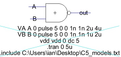
2) create a new cell schematic and name it NAND_gate_sim
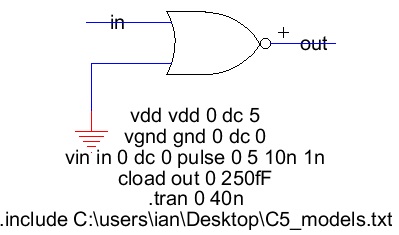
3) change A input name to "in", connect a power source to B, and change the output name to "out"
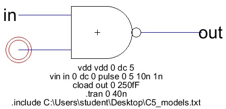
4) place spice code, schematic should look as follows:
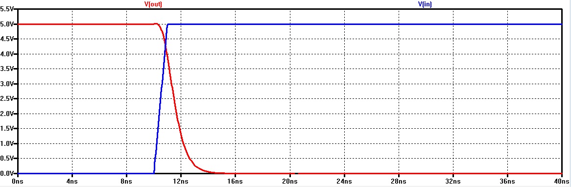
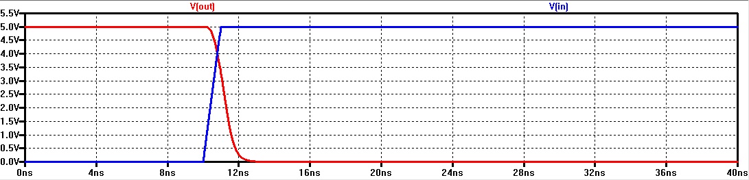
5) simulate and get the following results
Layout:
1) duplicate the inv_20_10 layout and name it NAND_gate
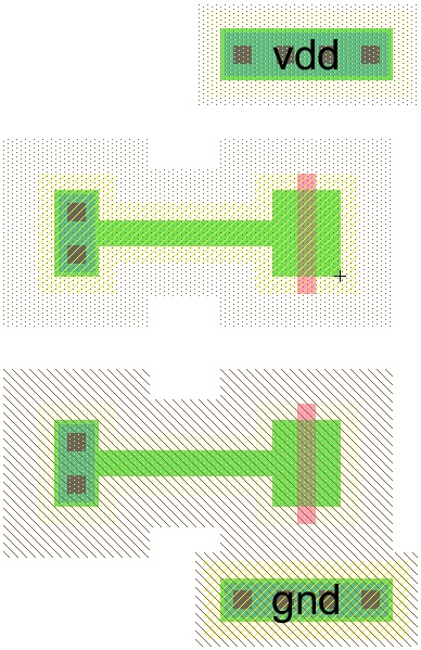
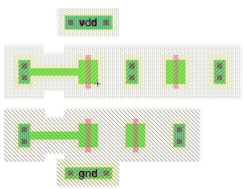
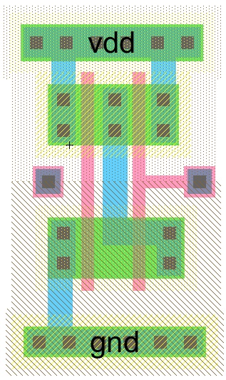
2) delete the arcs, pins and exports until you just have the following
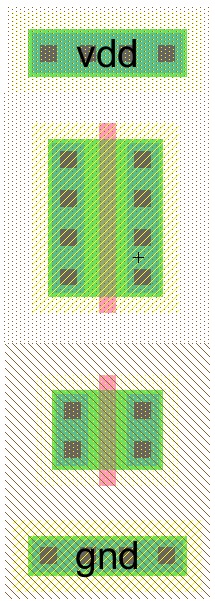
3) move the pAct and nAct out of the way and delete the corresponding side
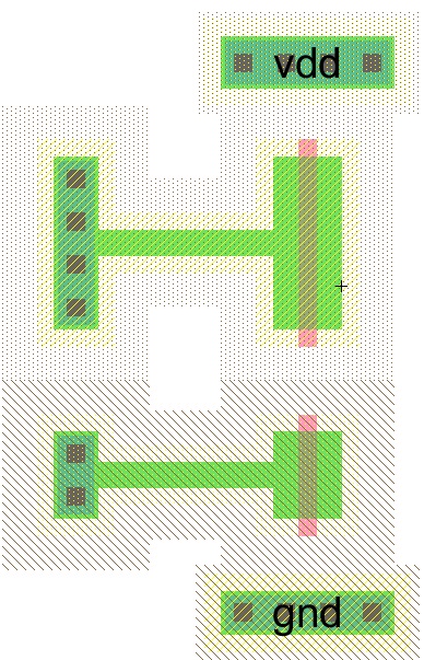
4) change the width and y-size of the PMOS node to 10
5) copy and paste the pACT node twice, and the PMOS node, NMOS node, nACT node once
6) add the arcs and move them together to compact it
7) add metal1 connections
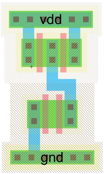
8) add metal1-poly1 contacts
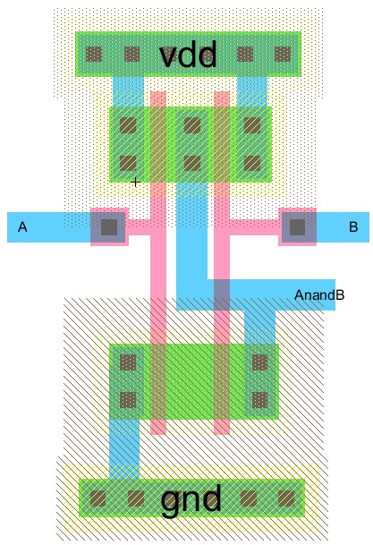
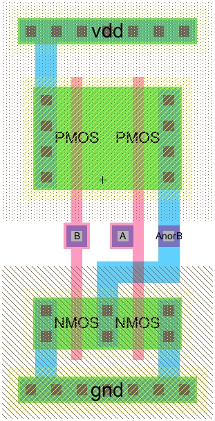
9) export the inputs A,B,AnandB as seen as follows
Gate Inputs:
1) create a new schematic and name it "NAND_gate_inputs"
2) copy over the icon view and create the A, B, out pins
3) write the spice code as seen below
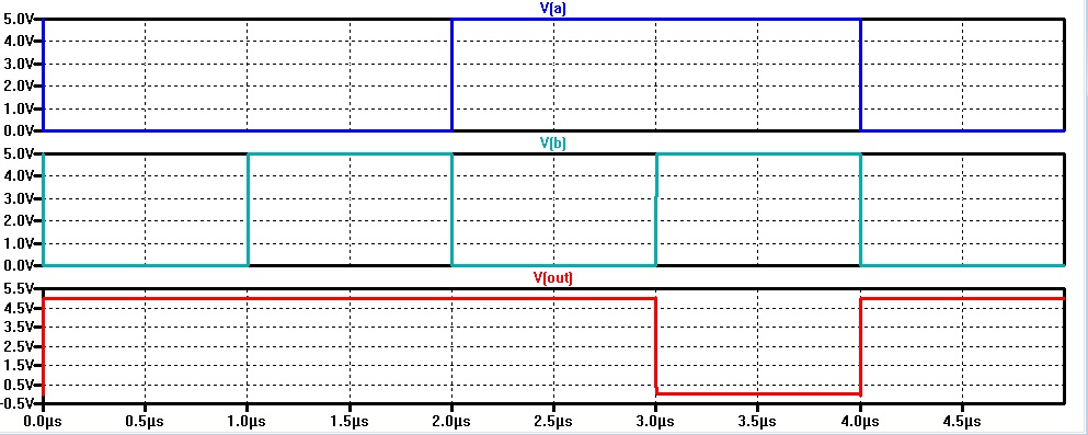
4) simulation results seen below
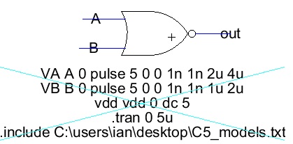
NOR gate
1) repeat all the steps above but for a NOR gate
Schematic:
1) copy the NAND gate cell group
2) change the PMOS width to 2 and length to 20
3) create the following schematic
Icon
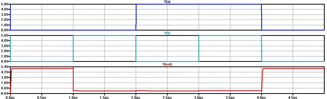
Simulation
Layout
Gate Inputs:
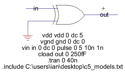
XOR gate:
Schematic

Icon View
Simulation