Lab 5 - ECE 421L
Lab
Use different methods: SPICE, ALS, IRSIM to simulate 20/10 and 100/50 inverters
- Go over Tutorial 3. The jelib file for tutorial 3 can be downloaded here
Inverter 20/10
1) Create a new cell and name it inv_20_10
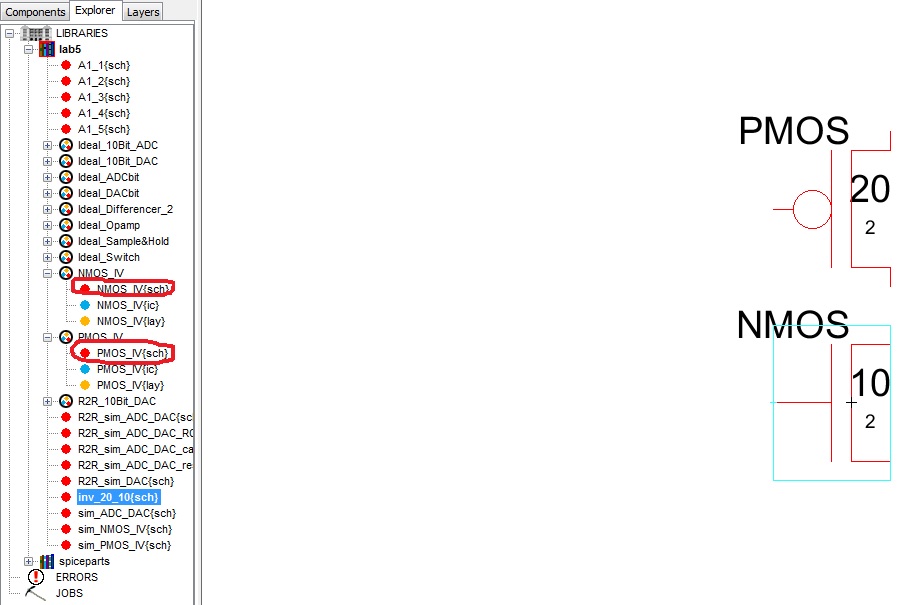
2) From the previous labs, copy and paste the NMOS transistor (NMOS_IV) and PMOS transistor (PMOS_IV) onto this new cell
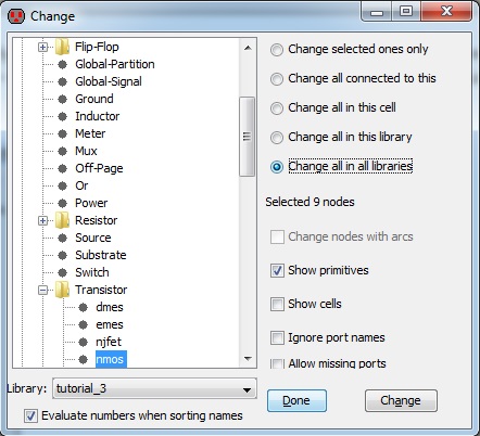
3) select the NMOS node and go to Edit->Change and change the Node to transistor and repeat for PMOS
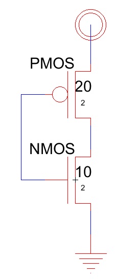
4) change the width of the PMOS to 20 and NMOS to 10 (CTRL+I)
5) add a power source (you can edit the size of the power source by pressing ctrl+b)
6) now add a ground
7) connect the components by adding wires as seen below:
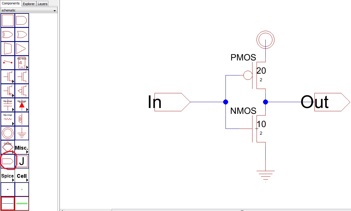
8) add off page nodes and export them as the inverter's input and output (In being left, Out being right) and connect the wires
Making the icon
1) go to View -> Make Icon View
2) go to Explorer and double click the icon file
3) select the box and delete it leaving only the In and Out exports
4) select the Out export and move it to the right and using CTRL+J, rotate it so the wire points left
5) select the triangle from the components menu and drop it on the schematic, rotate it so it points right
6) select the circle from the components menu and drop it on the schematic so its at the end of the triangle
the icon should look like this
![]()
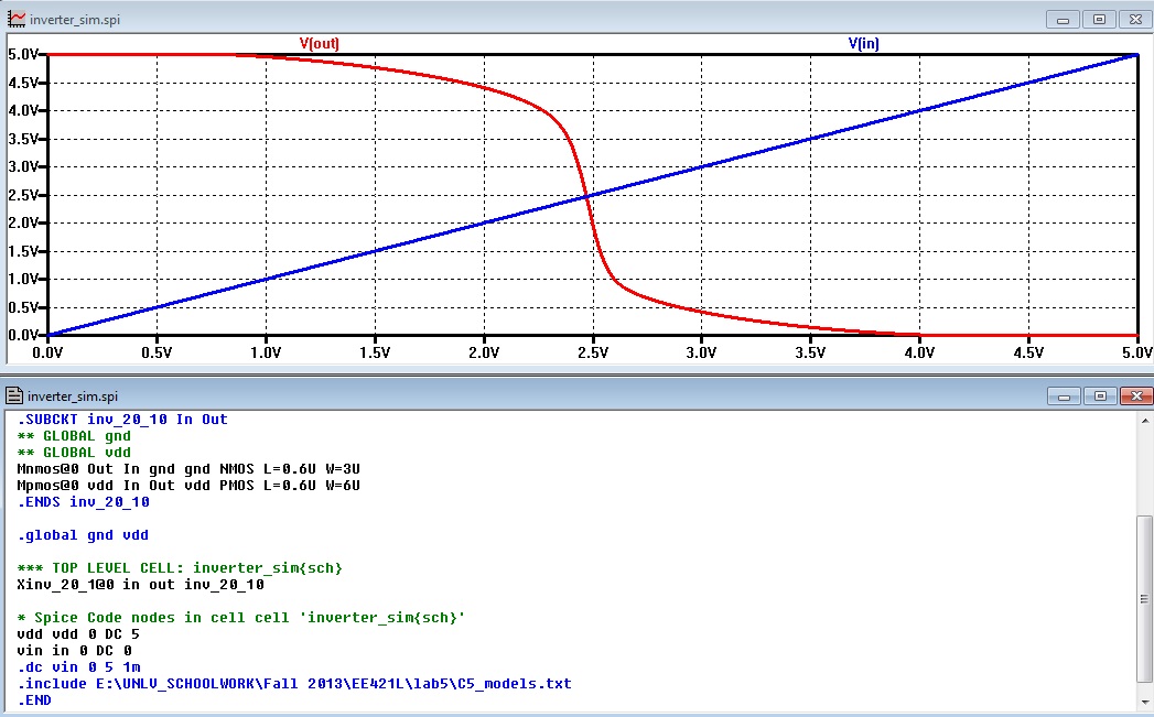
Simulation
1) Create a new cell schematic and name it the inverter_sim
2) place the icon into this new schematic
![]()
3) add wires to extend the in and out arcs
4) place the spice code as seen below

5) simulate to get the following:
Layout of inverter
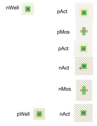
1) create a new layout cell and name it inv_20_10
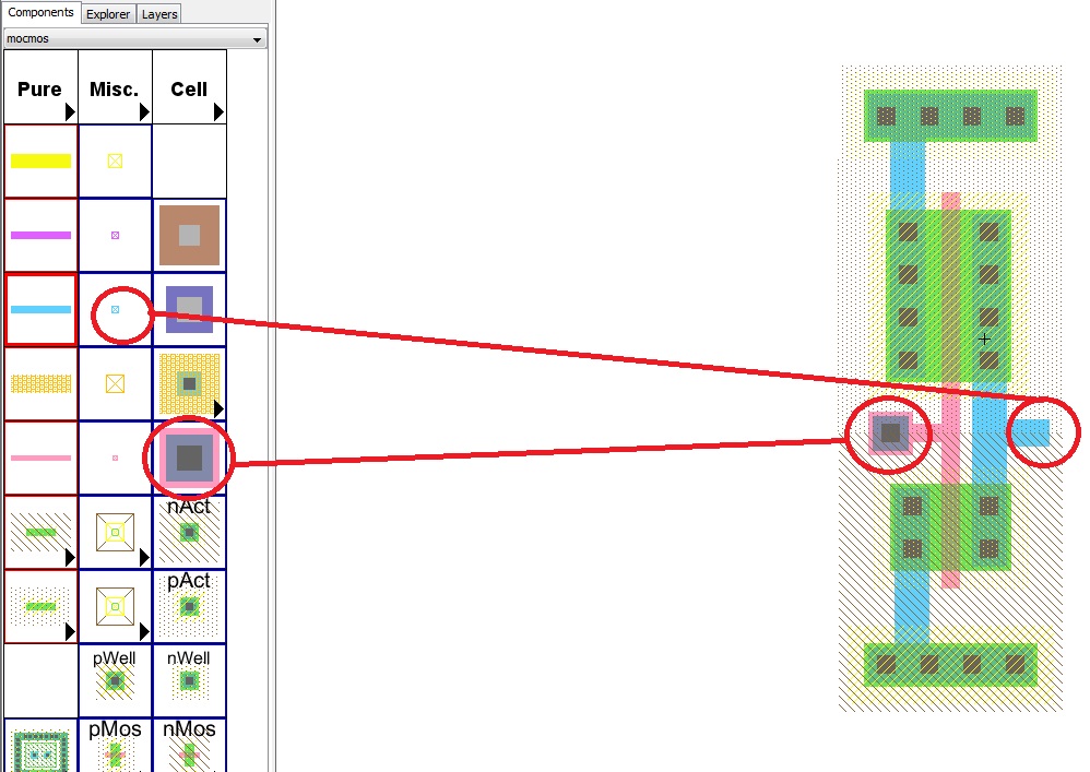
2) add the following nodes seen below
3) select the PMOS node and set the width to 20 and select the NMOS node and set the width to 10
4) set the x-size of the PACT nodes to 20 and the NACT nodes to 10
5) set the pwell and nwell x-size to 20
6) now add arcs between the transistors and active areas as seen below
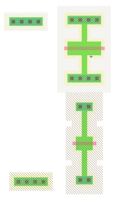
7) rotate the transistors and lign up the components as seen below
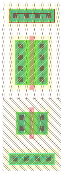
8) connect the transistors together and the metal connections as seen below
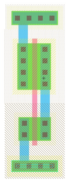
9) add a poly1 to metal1 contact on the left and a metal1 pin on the right as seen below, make sure the width of the poly is 2
10) export in, out, gnd, vdd
Creating an easier view for layout
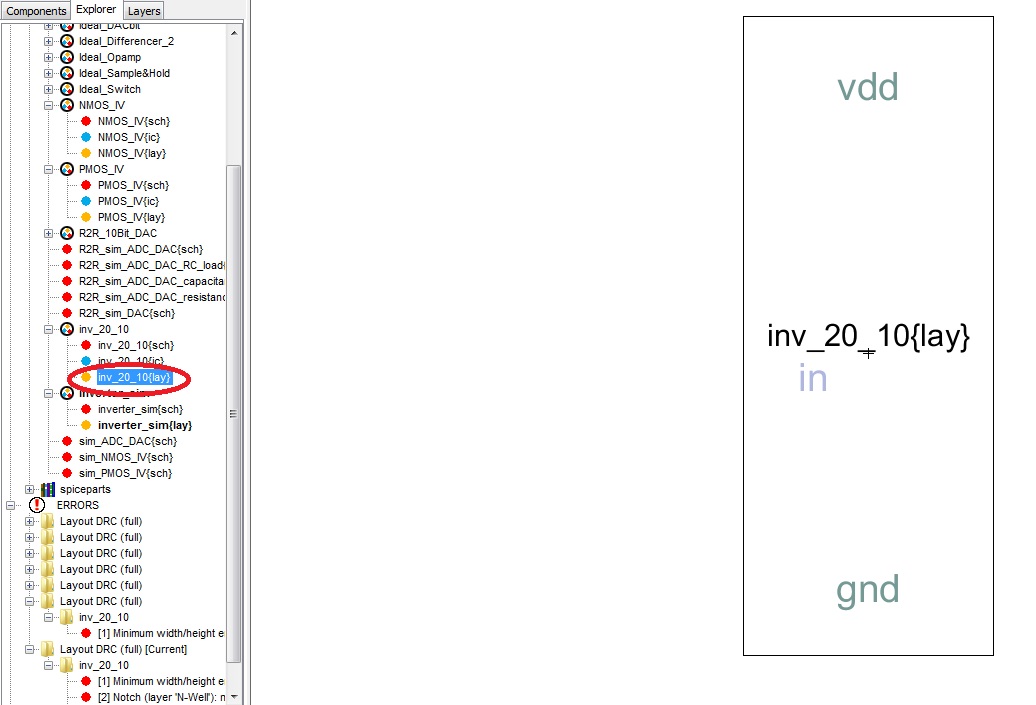
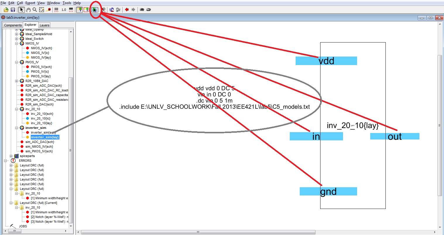
1) create a new cell named inverter_sim with a layout view
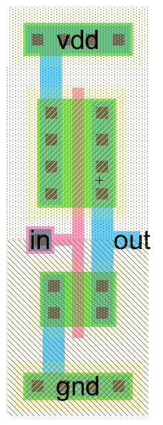
2) in the explorer, drag inv_20_10{lay} over into the drawing area of inverter_sim{lay}
3) select the special select tool and click on each node and add a metal1 arc
4) rename the arcs to its corresponding names
5) copy the spice code from the schematic and place it into the layout
6) DRC check and you will get 2 errors, to get rid of these errors delete the vdd and gnd names from the arc
7) Export the left pins on the top and bottom metal1 Arcs with names vdd and gnd
8) DRC, NCC, Well check with no errors