Lab 3 - ECE 421L
___________________________________________________________________________________________________
Lab
Description:
Discuss how to select the width and length of the resistor by referencing the process information from MOSIS
-To select a width, we look at the design rule which states that the minimum width is 12
- By selecting a width of 12, and the sheet resistance is 800 ohms, to find the length we simply
derive L from the equation resistance equation:
R = Rsheet * (L / W)
-Finding L in this equation gives us:
L= R * W / Rsheet
-plugging in the numbers, we get
L = 10,000 * 15 / 800
and we have L = 187.5
- For each of these resistors, using a width of 12, the dimensions of the resistor becomes 12 by 150 and the total resistance is 10k
ohms because of the equation:
R = Rsheet * (L / W)
10000 = 800 * (187.5 / 15)
Designing a DAC layout and use the n-well node for the layout of a 10k resistor
1) Create a new cell layout and call it "R_divider"
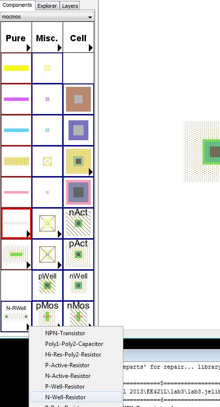
2) Select the N-well resistor in the components tab in the Explorer as seen below
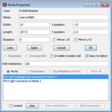
3) click on the resistor and press ctrl+i and edit the values for length=187.5 and width=15 and a resistance of 10k
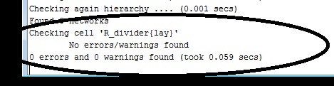
4) Press F5 to check if there are any errors
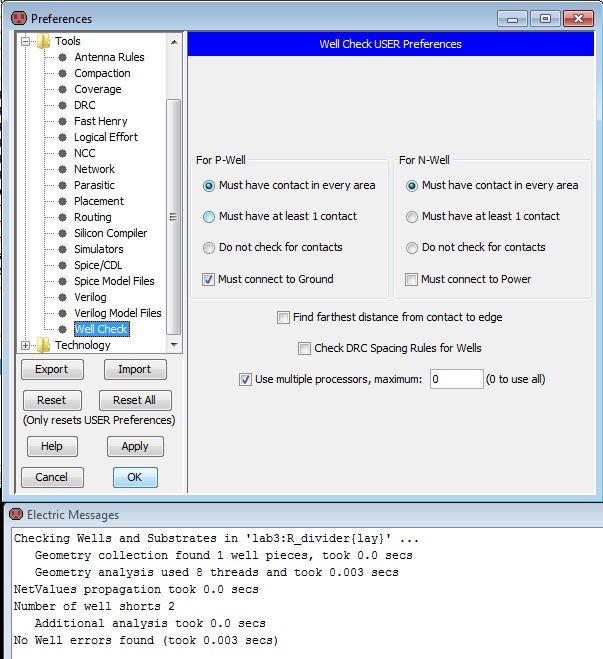
5) ERC is to verify that the p-well is always connected to ground in C5 process as used in the tutorial.
To setup the ERC well check go to Preferences -> Tools -> Well check
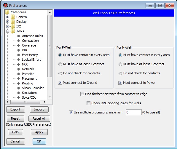
6) Now go to Tools -> ERC -> Check Wells
7) You will see that you get an error, that is because for the N-well resistor it does not need to be connected to Power
so uncheck that box and check wells again and it will not have any more errors
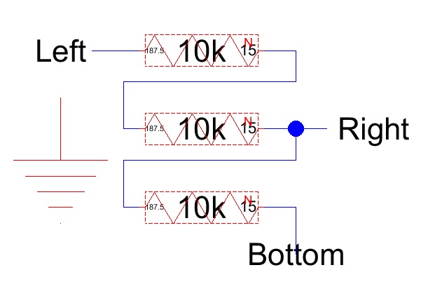
8) Now lets create the resistor schematic
9) Create a new cell schematic and call it "R_divider"
10) using the n-well resistors create the following circuit
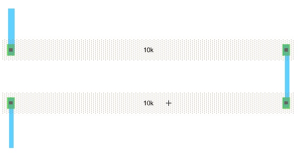
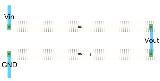
9) Now lets create the layout for the resistor, go back to the previous layout
10) Copy and paste the resistor to make 2 resistors total and line them up
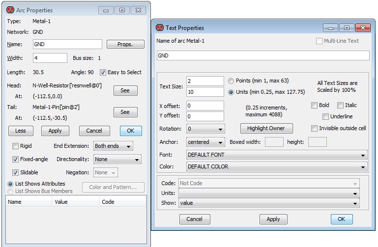
11) Using metal1 connection, create the following
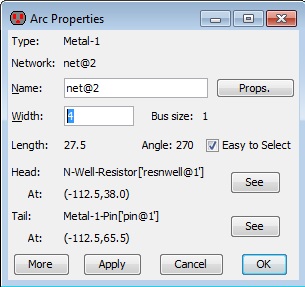
12) cchange all the arc widths by pressing ctrl+i to change the width to 4
13) Label all the arcs Vin, Vout, GND by pressing ctrl+i and changing the names to the appropriate names
Click on Props to change the text size to 10 units
14) You will have the folowing layout
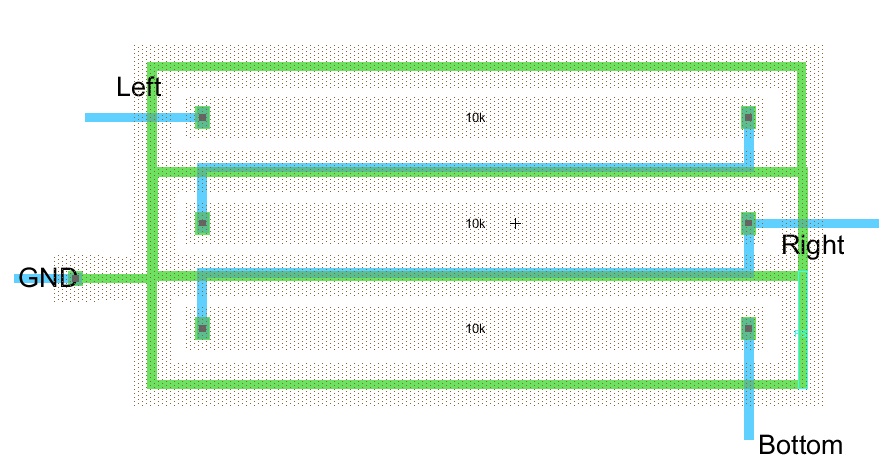
15) Using this layout, lets create the following layout
16) back up all work
The Electric Library for Lab 3 can be downloaded here LAB3