
Lab Project - EE 421L
Edgar Solorio
A AND B


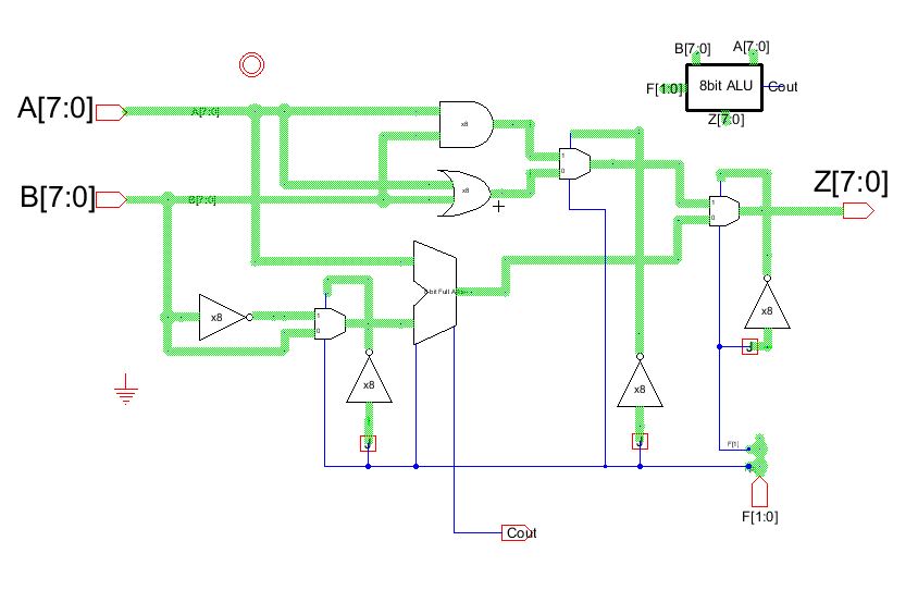

The operation of the ALU is pretty simple, the first thing to note is
that there are three 2-to-1 MUXes used at the right side of the schematic
to create a single 4-to-1 MUX. The 2-bit "F" input (F for function) controls
which part of the circuit will be outputted to "Z" an 8-bit output bus.
The following truth table describes what function is done with all four
combinations of the input "F".
| F1 | F0 | Function |
| 0 | 0 | A + B |
| 0 | 1 | A - B |
| 1 | 0 | A OR B |
| 1 | 1 | A AND B |
The AND operation of the ALU is simply done by inputting A and B into the
8-bit AND gate, the output then enters as an input to a mux which then the
output of that mux enters as an input to the last mux. If the "F" input is set
to "00", then the AND operation between "A AND B" is outputted to Z.
The same process occurs for doing "A OR B", except the "F" input has to be
set to "01".
For addition and subtraction, there is another MUX used to select between
B or ~B (where "~" denotes the inverse). Addition simply works by passing A
into the Full Adder and by letting B pass into the FA as well. B is chosen since
the combination of the input "F" is "00", where F0 would then select input 0
from the MUX that gates the input B into the ALU.
For subtraction, we need to understand how numbers are subtracted in 2's
complement to see why the design is set up the way it is.
"A - B" is the same as "A + (-B)" where "-B" is the negative number of B.
In order to achieve "-B", we simply invert all the bits in "B" and add 1.
-B = ~B + 1 for a 2's complement representation. Notice that when "F"
is set to "01" (F0 is equal to "1"), the F0 signal is fed into the carry in
of the FA to provide the "+1". The F0 also selects the input from selection
1 of the bottom left MUX of the schematic, which negates B to create ~B.
Therefore, subtraction is done by having "A + (~B) + 1" which is equivalent
to "A - B".
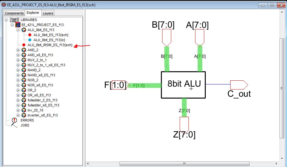
Simulation using IRSIM -
The next step was to simulate my design to make sure it functions as it should,
I created an icon view and a new schematic cell called "ALU_8bit_IRSIM_ES_f13"
to simulate the 8-bit ALU as seen below.

I started IRSIM on the schematic from above and input the following waveforms to
demonstrate the operation of the A AND B function, when F[0:1] = 0x03.
Note that the operation is correct, but there is a hiccup at about 4us when the input
B is transitioning. The output can be seen at the bottom, signal Z[0:7].

The next operation to simulate was the A OR B function, when F[0:1] = 0x02.
Notice again that the operation is correct except for when the inputs A and B
are transitioning.

The next operation I simulated was A - B, when F[0:1] = 0x01.
I set A = 93 (0x5D) and B = 28 (0x1C), the result is Z = 65 (0x41).
The simulation has some jitter to it between 1.5 ns and 4.2 ns but
then settles to the correct value of 0x41 as shown below.
Note that A[0],B[0], and Z[0] are the lowest significant bits in the 8-bit number
and that A[7],B[7], and Z[7] are the most significant bits.

The final simulation was the A + B function, when F[0:1] = 0x00. I put in simple test numbers
and set A = 11 (0x0B) and B = 96 (0x60) gives me the expected result of Z = 107 (0x6B).
Notice again that the circuit needs time to settle to the final value of 0x6B as shown below.

BACK-UP! -
As always, back up your work in case of a disaster or stray EM pulses.
A copy of my project jelib can be found here.

In part 1 of this lab project, I went through the process of creating an 8-bit ALU
with two inputs using 8-bit components (such as inverter, AND, OR, MUX, and FA gates).
I also tested out the schematic using IRSIM to verify that it indeed operates successfully.
In part 2 of this lab project, I will go through the process of laying out the 8-bit ALU.
I first start by laying out all of the 1-bit gates (NOT THE 8-BIT VERSIONS!).
To make the layout more compact, I created a standard frame cell as shown below
to keep well area sizes the same for all gates.
 From this standard frame cell, I can put each gate in the area and simply resize the
1-BIT AND GATE

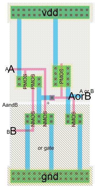
1-BIT OR GATE
1-BIT MUX GATE (2-to-1)

1-BIT FULL ADDER

The next step was to create the 8-bit ALU one bit at a time. In the images
below, each gate that was layed out was put side to side in this order:
Inverter -> Inverter -> MUX -> AND -> OR -> Inverter -> MUX -> FA -> Inverter -> MUX
The first image has the internal components hidden, the second image has
all the components shown, and the third image shows how all the components
were interconnected.


By having this 1-bit ALU string, it makes creating the overall 8-bit ALU easy by
simply copy and pasting the 1-bit string 8 times as shown below, but with
minor changes in interconnections to account for carry outs flowing into the carry
ins of the next bit for example.

As shown in the annotation text above, the overall layout spans 1492 by 951 lambdas.
The complete layout was then DRC'ed, NCC'ed, and Well checked to
show that is has no errors.

BACK-UP! -
As always, back up your work as shown below.
A copy of my project jelib can be found here.
