Lab 7 - ECE 421L
Edgar Solorio,
solori12@unlv.nevada.edu
November 1, 2013
Lab
description
- Finish Tutorial 5, and learn how to use the buses and arrays for circuit simulations.
- Use buses and arrays in the design of word inverters, muxes, and high-speed adders
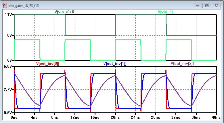
Below we have an 8-bit inverter and I simulate its driving capabilities with different
capactive loads, notice that it cannot drive a 1pF capacitor quickly.
8-Bit Inverter


In order to create an 8-bit ALU, we need to create an 8-bit NAND, NOR, AND, and OR gates
(we already created the 8-bit Inverter). Our ALU will have 2 inputs, so all of our gates will be 2
input gates as well, I start off by creating simple 2-input gates as shown below.


Now by using the skills acquired from Tutorial 5 (by using buses and arrays), I can create an 8-bit version of each
2 input gate as shown below with the corresponding icon shown on the top right of each gate.


Now it's time to simulate all of the 8-bit 2-input gates in the same schematic
cell as shown below. Note that three capacitors are tied to 3-bits of each gate
to test out how fast it can drive a capacitive load. Below is the schematic cell,
and a zoomed in view of how it is laid out.


The simulation results for all 5 gates are shown below with no loads attached to the outputs

I know test each 8-bit gate with three various capactive loads that were shown in the schematic cell
that contains all 5 gates that was previously shown.
8-bit AND gate (2-input)

8-bit INVERTER gate (2-input)
8-bit NAND gate (2-input)

8-bit NOR gate (2-input)

8-bit OR gate (2-input)

We have most of the components necessary for the creation of an 8-bit ALU, the
final thing needed is a component called the DEMUX. What the Demultiplexor (DEMUX)
does is it takes in multiple inputs and routes one of those inputs to the output by using the
select signal. The result is thus Out = a*select + b*select_inv. The mux is helpful for connecting
multiple inputs to a bus and only letting one input through at a time. The DEMUX is simulated
below with the following circuit, notice that "a" is tied to ground and "b" is tied to 5 volts.
The select signal is a clock source input.


If the multiplexor can accept multiple inputs and send it to a single output, can it
take a single input and pass it out to multiple outputs? The answer is yes and this
component is called a Multiplexor (MUX). It is essentially the same as a DEMUX,
but mirrored Left to Right, a simulation schematic is shown below. Notice that our
input is a fast frequency signal and our select signal will choose where the input will
be routed to either output A when select is 1 or output B when select is 0.


Now that we know our 2-input MUX/DEMUX unit works correctly, we need
to make it into an 8-bit gate like previously done with the other gates. Notice
that an inverter is used to provide the select_inv signal.

To simulate the new 8-bit MUX/DEMUX gate (which I will from now on
just refer to as DEMUX) I tied the first 3 bits of A to VDD and the first
3 bits of B to GND as shown below. A simulation is shown as well, notice
that when vsel is set to VDD, the outputs out[7], out[6], out[5] are the
same as VDD, since A[7], A[6], A[5] are being passed through.
The outputs are GND otherwise.


We can also verify that the DEMUX/MUX works from a logical level
by using IRSIM to verify the results. The following are the schematic
cells followed by IRSIM results for both the DEMUX then the MUX.
DEMUX W/ IRSIM - When The Select signal is "HIGH" (the voltage is vdd)
the fast frequency signal at input A is passed through to output, when the
Select signal is "LOW" (the voltage is at gnd) the output is "LOW" since B is tied to gnd.


MUX W/ IRSIM - For the multiplexor simulation, I create a fast
frequency input signal. When the select signal is "HIGH", the input
signal goes to output A; when the select signal is "LOW", the output
signal goes to output B as shown below.


DEMUX (8-BIT) W/ IRSIM - This is a quick simulation of the 8 bit DEMUX circuit.


Now we will draft the schematic for a full-adder as seen in Fig. 12.20
from the CMOS textbook. The PMOS and NMOS devices have size 6/2
as shown below (with the icon on the top right shown).

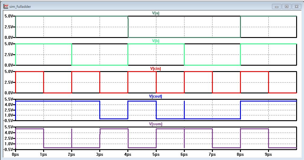
We will now simulate our Full-Adder circuit, the truth table for
the full adder is shown below followed by the simulation schematic
and simulation results.


I know create an 8-bit version of the 2-input Full Adder as
shown below with the icon shown at the top right.

A simulation of the 8-bit Full Adder is shown below. The schematic
shows the addition of two numbers and what the result should be for
each Sum[7:0] bit. Notice that the simulation results show that only
output Sum[7], Sum[6], Sum[5], and Sum[4] are "HIGH", which means
the numbers were correctly added. Refer to the schematic image for
more information given by the notes.


The final part of this lab is to create an 8-bit adder with the schematic
given by Fig. 12.20 using 6/2 devices. The image below is the 2-input full
adder which will be used as the building block for the 8-bit full adder.
I NCC, DRC, and Well check the layout and pass without errors as shown.


The 8-bit full adder is shown below along with passing the
NCC, DRC, and Well checks as before and that concludes lab 7.


BACKUP YOUR WORK!!!
A link to my lab7 jelib is found here as well lab7_jelib

Return to EE 421L Labs