Lab 4 - EE 421L
Authored
by: Medhanie Petros
E-mail: petrosm@unlv.nevada.edu
Date: 9/27/2013
Lab
description
1. Pre-lab work requires to finish Tutorial 2.
2. Backup the lab report and upload it to the CMOSedu.com for future study and discussions.
Postlab # 4
To begin save this library as tutorial_2.jelib in C:\Electric.
Next save the file C5_models.txt to C:\Electric for SPICE simulations. This file contains the MOSFET models for the C5 process.
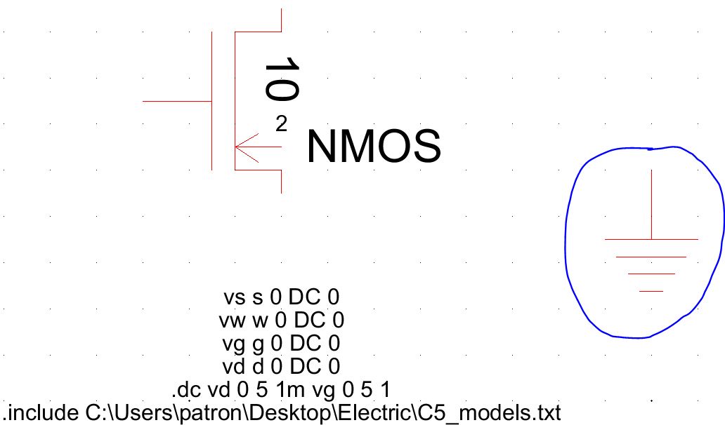
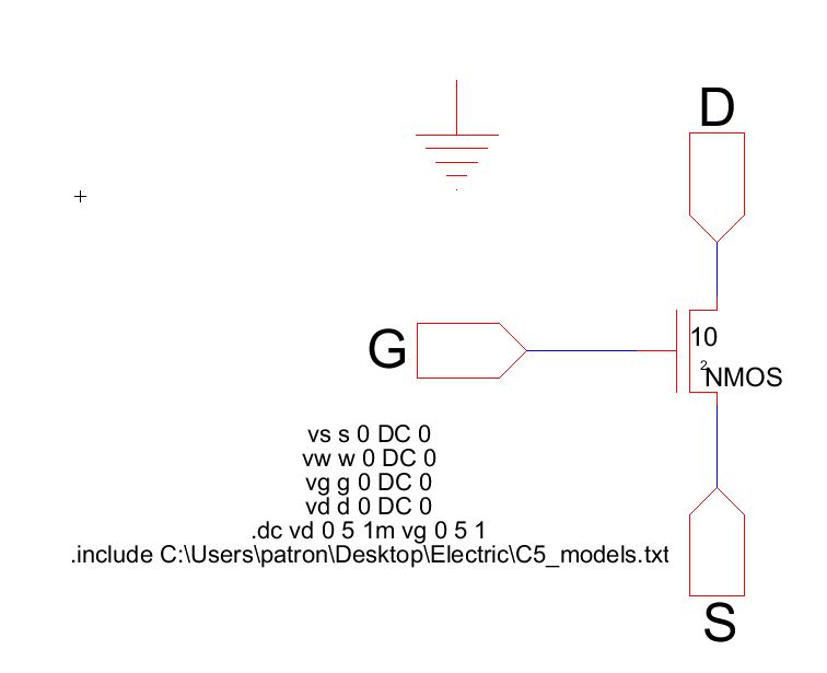
When finished create new cell, a schematic called NMOS_IV, see below.
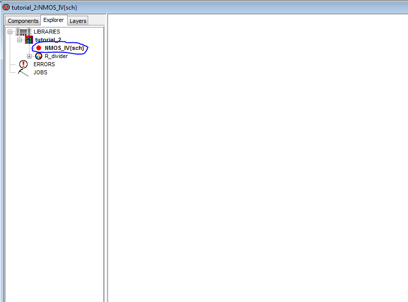
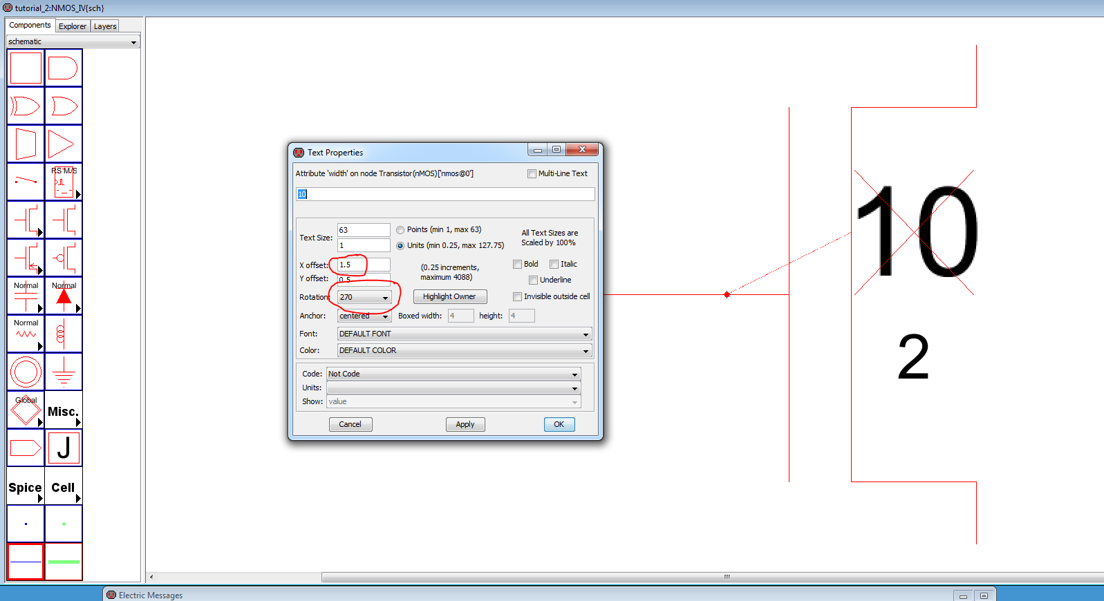
Next go to the componets window and select/ place the NMOS Node. Then Edit the Nodes properties;
Set the with of the device to 10 and leave the lenght at 2.
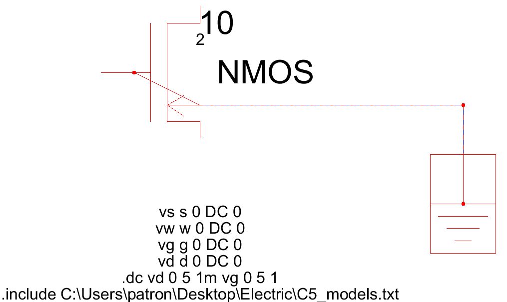
Next, select the NMOS Node and go to Tools >>> Simulation (Spice) >>> Set Spice Model;
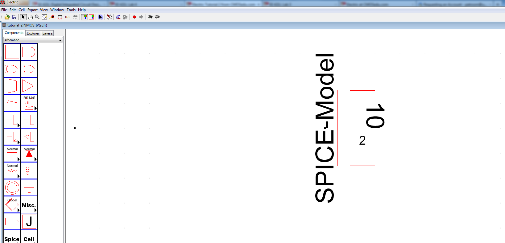
Edit the SPICE-model text using Ctrl+I from
the C5_models.txt file above we see that the NMOS model name is NMOS
and the PMOS model’s name is PMOS. Change the name to NMOS and
Rotation to 270 as seen below.
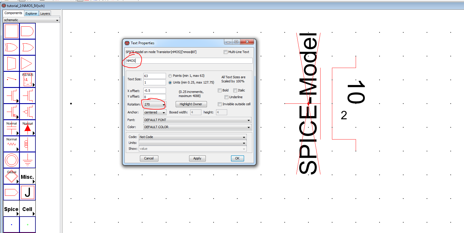
After you move the SPICE name to the right side position,
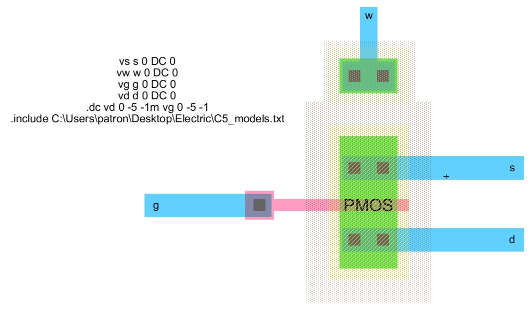
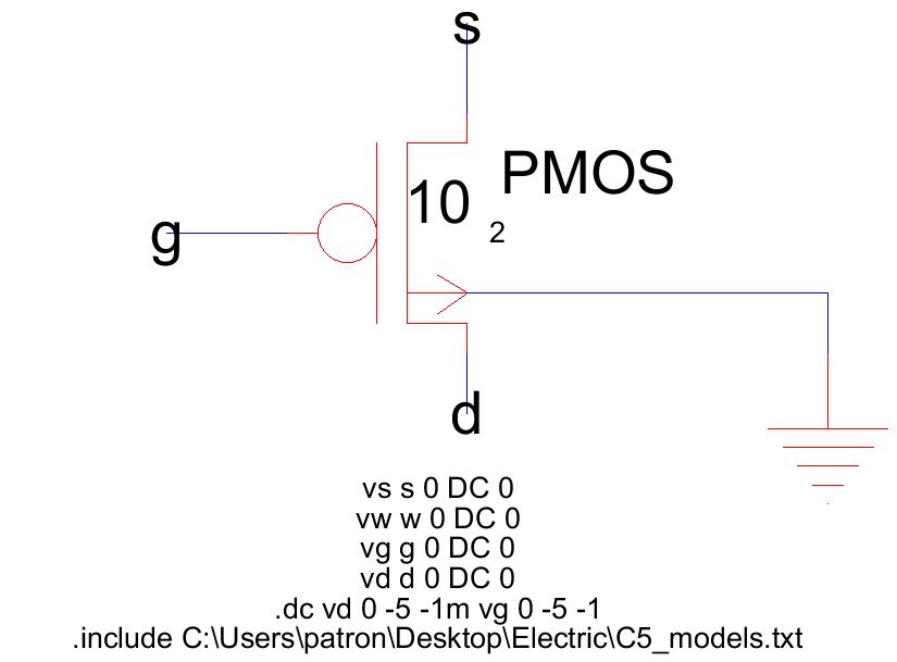
Repeat all the above steps for the PMOS device.
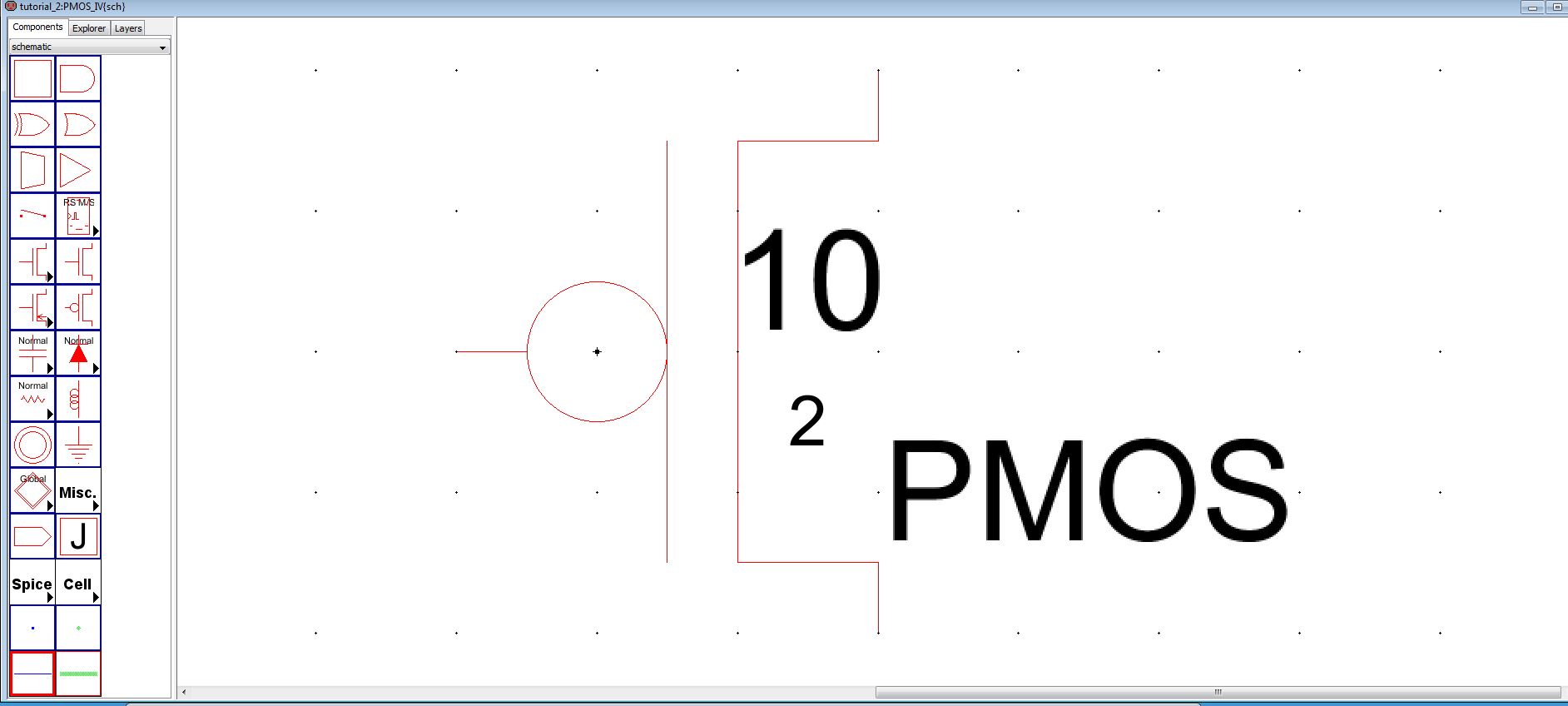
The cell name should be PMOS_IV.
The result is seen below.
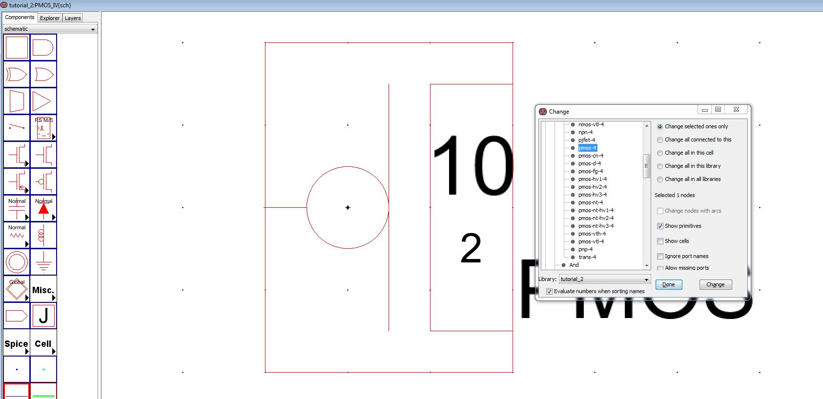
In this PMOS_IV cell select the PMOS Node then go to the menu Edit >>> Change or simply press C
Change the Node to a 4-port device as seen then Apply and Done.
Do the same thing for NMOS too.
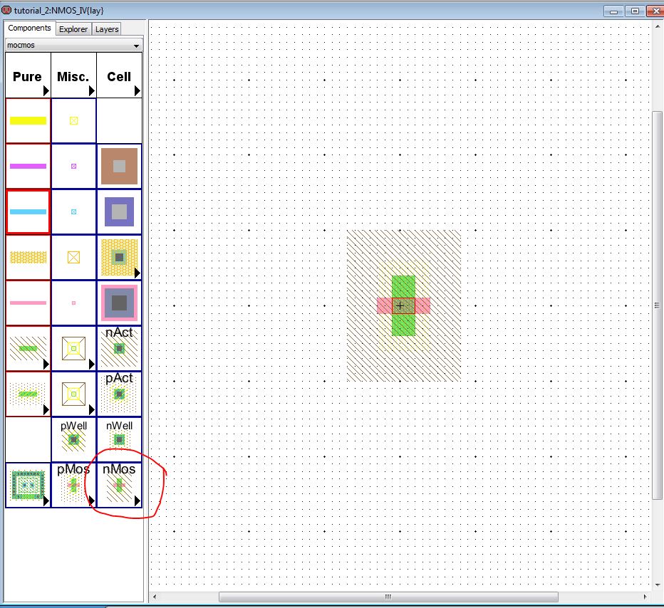
Next creat these two cells now by going to cell >>> New Cell
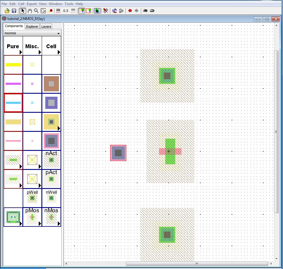
Go to the components menu on the left and select/place the nMos Node in the lower right corner of the menu
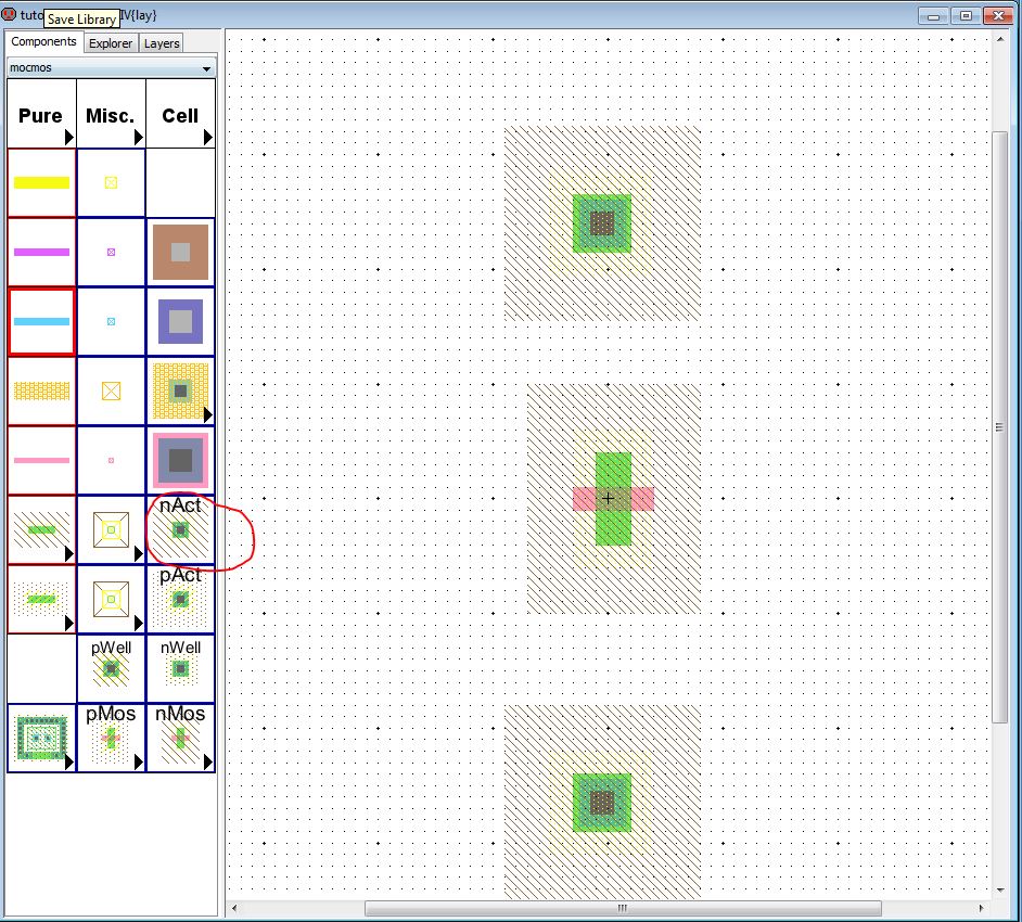
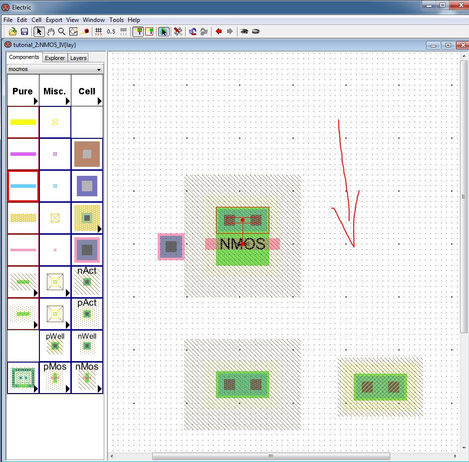
Next add nAct Nodes as seen below.
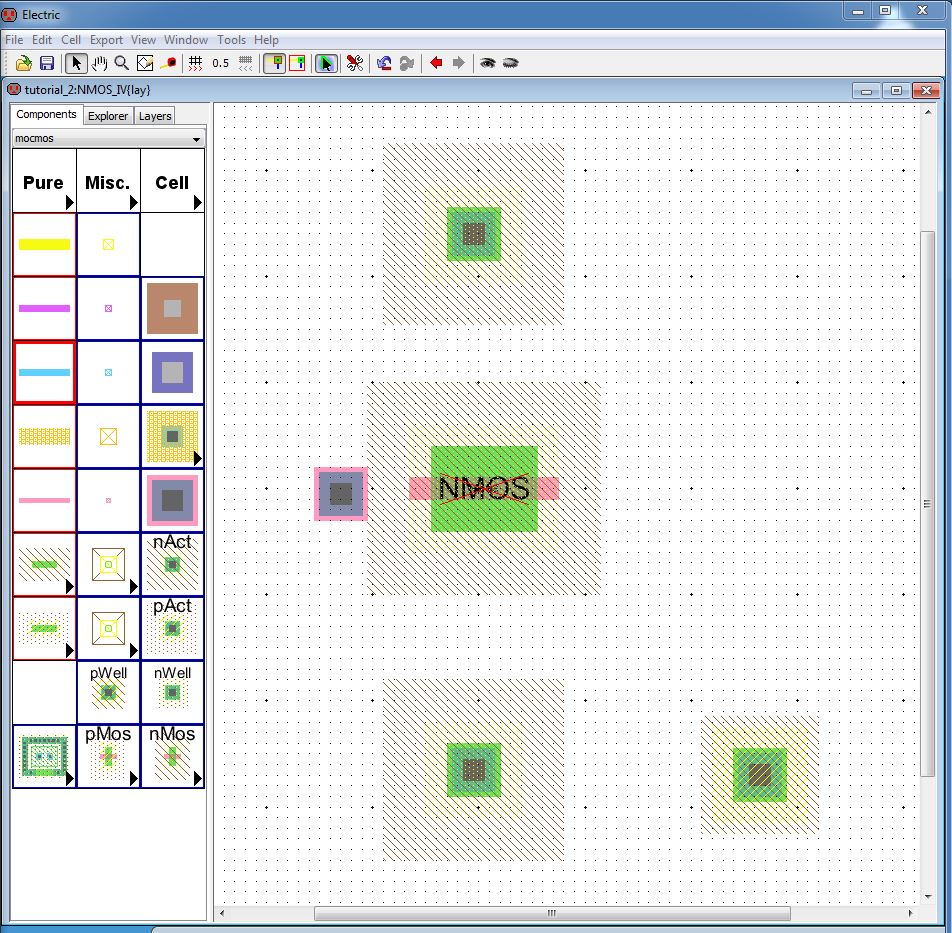
Next add the metal1 to conect to poly1 as seen below
Place the body connection for the NMOS device, the pWell Node seen below.
Zoom out as needed.
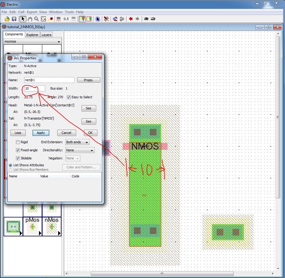
Next select both of the nAct Nodes.
Change the X size to 10, the same width as the MOSFET.
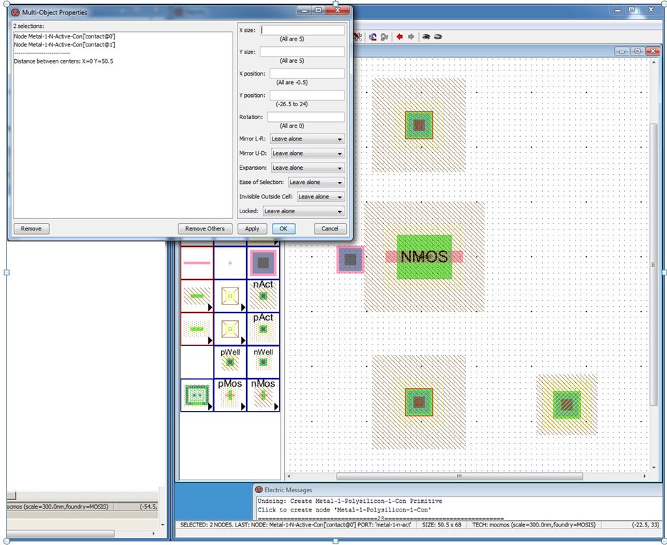
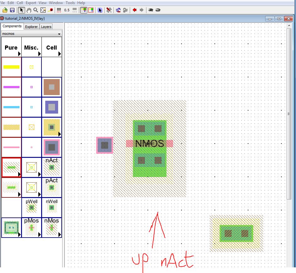
Move the mouse up to top nAct Node and RIGHT click on it.
At this point move the nAct Node down to match the following.
DRC your layout, F5, after you’ve moved the Node to ensure no design rule errors.
If we keep moving this Node the n-Active Arc will eventually move as well.
This behavior is related to the Arc’s properties.
Selecting Rigid will make the Arc move when we move the nAct Node.
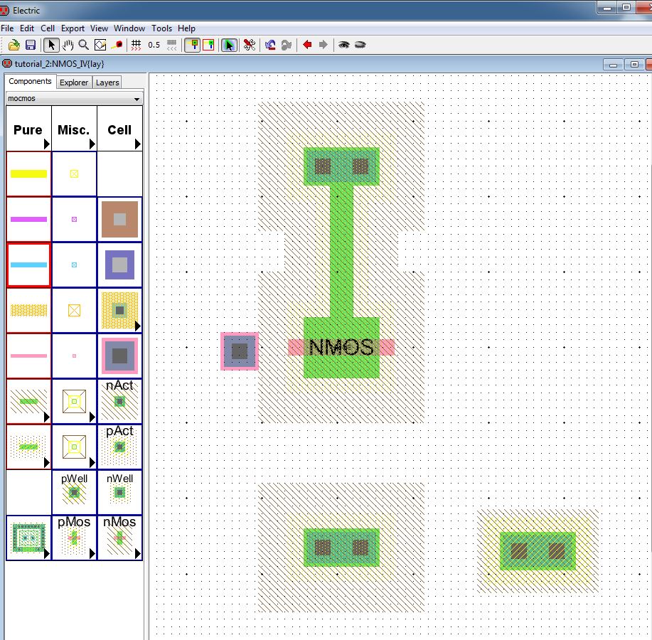
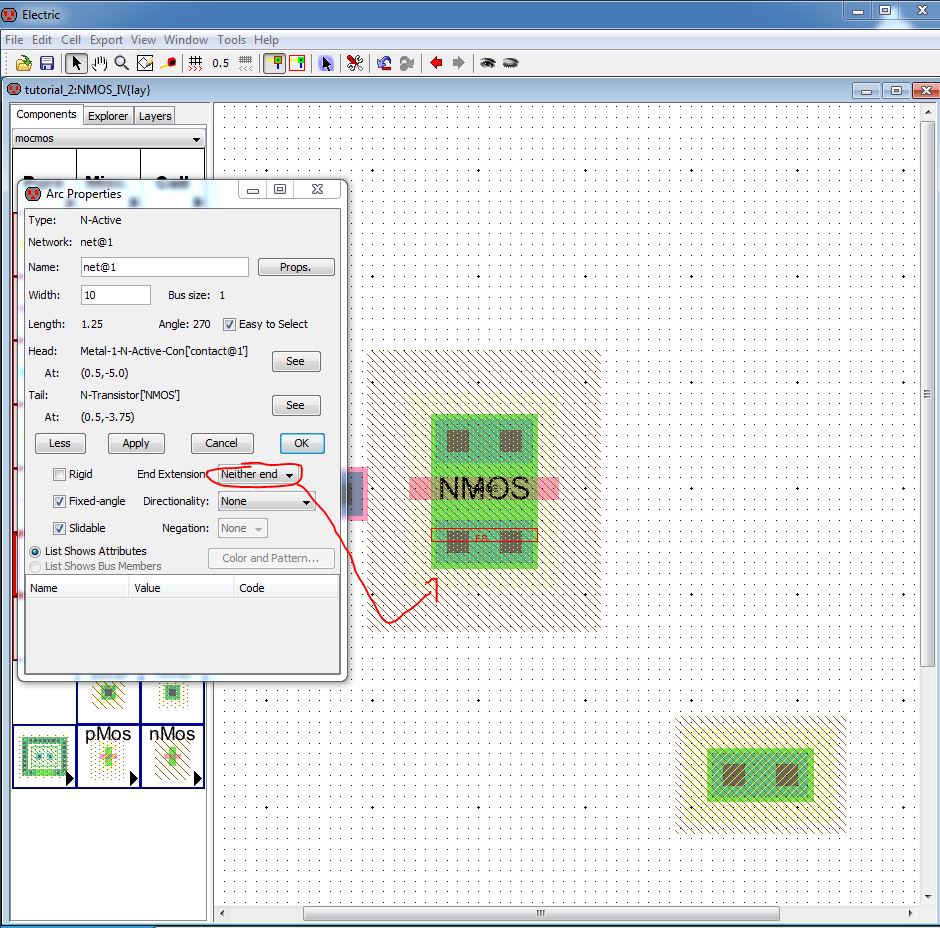
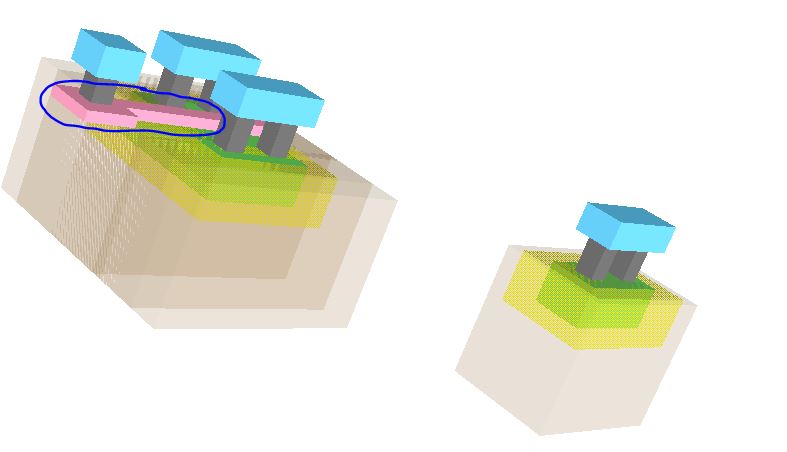
Move the bottom nAct Node up into place and DRC the layout.
echange this Arc's properties so that the end extention is "Neither end".
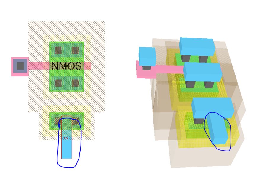
Moving the cursor over to the metal1-poly1 contact and RIGHT clicking gives the following, (Note that the fig below is in 3D).
DRC the resulting layout to verify no DRC errors.
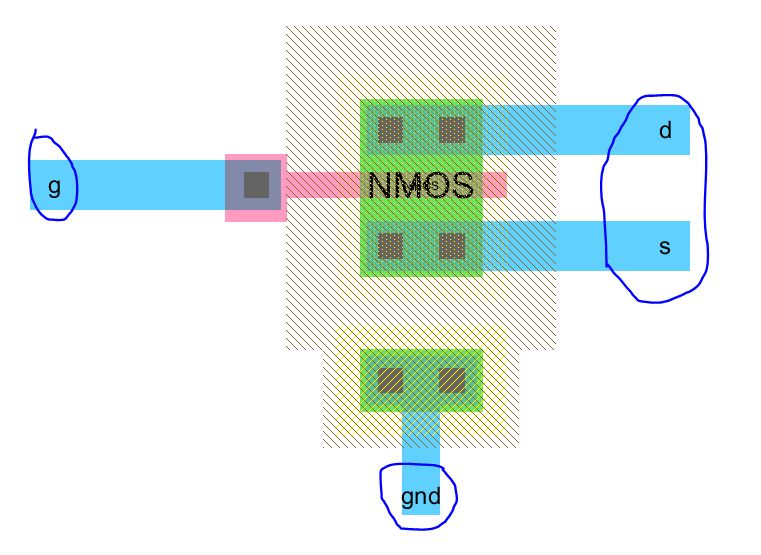
g
Move your cursor below the selected pWell node and right click to it
will look as following ( note that the other fig. is in 3D);
Next, with the pin selected, got to the menu and select Export >>> creat Export
Make sure to DRC and ERC-Check Wells when you are done.
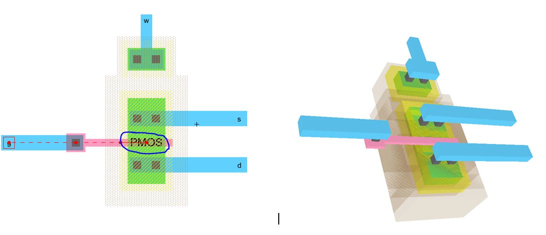
Follow the same sequence of actions to lay out the PMOS
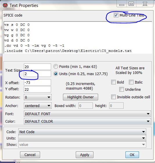
Go to the left component menu and select the arrowhead under Misc to access Spice Code.
And the cell would look like the following fig.
By going to the menu Tools >>> Simulation (Spice) >>> write spice Deck, the result will be as the following
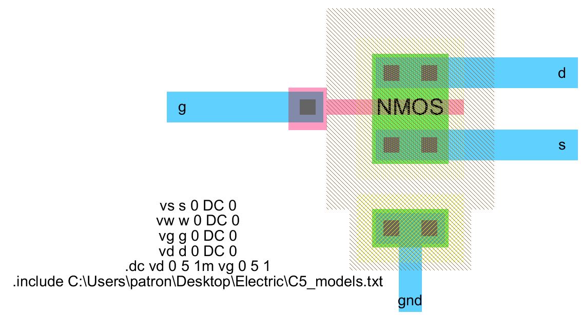
By doing the same process as PMOS to NMOS we get the following result;
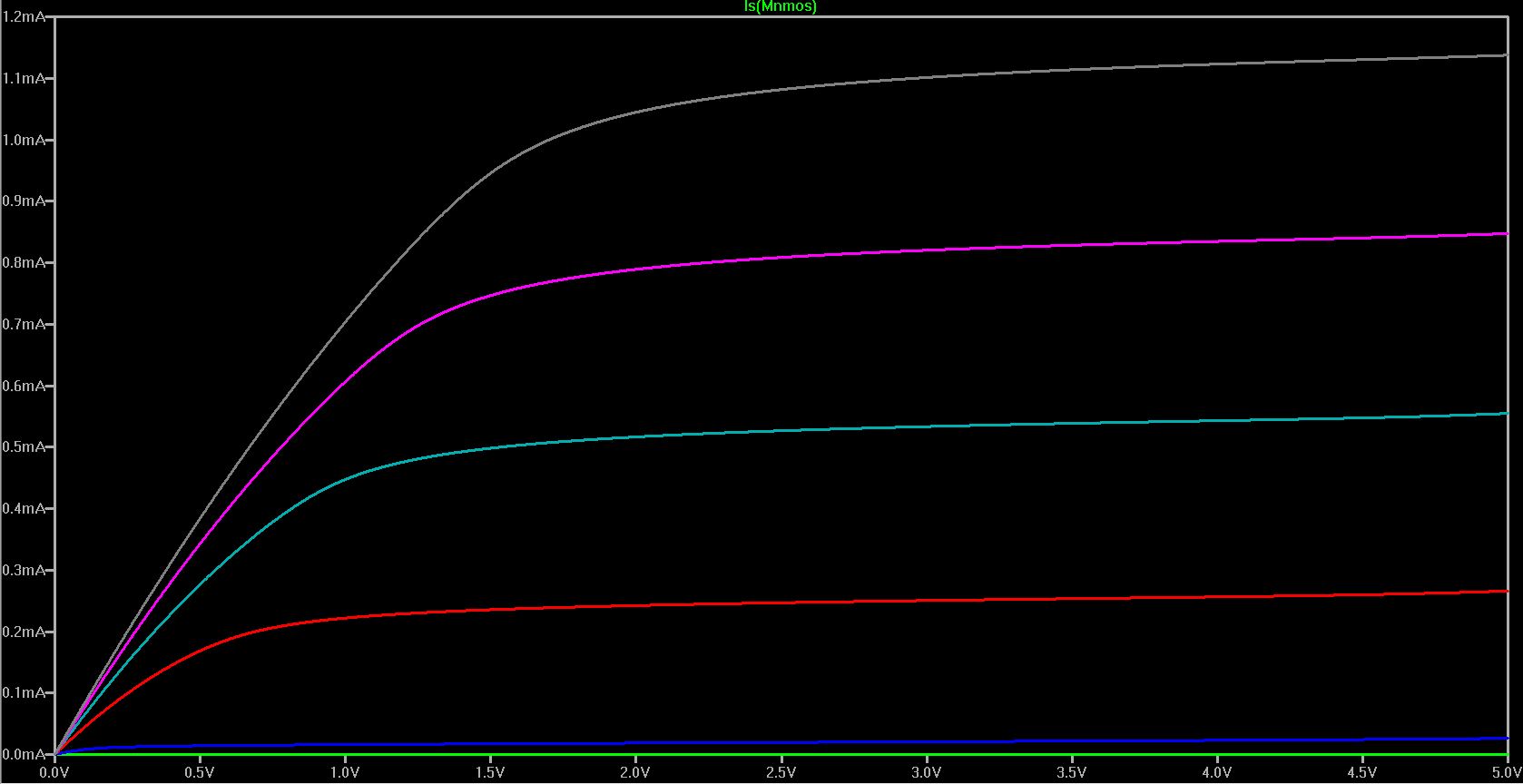
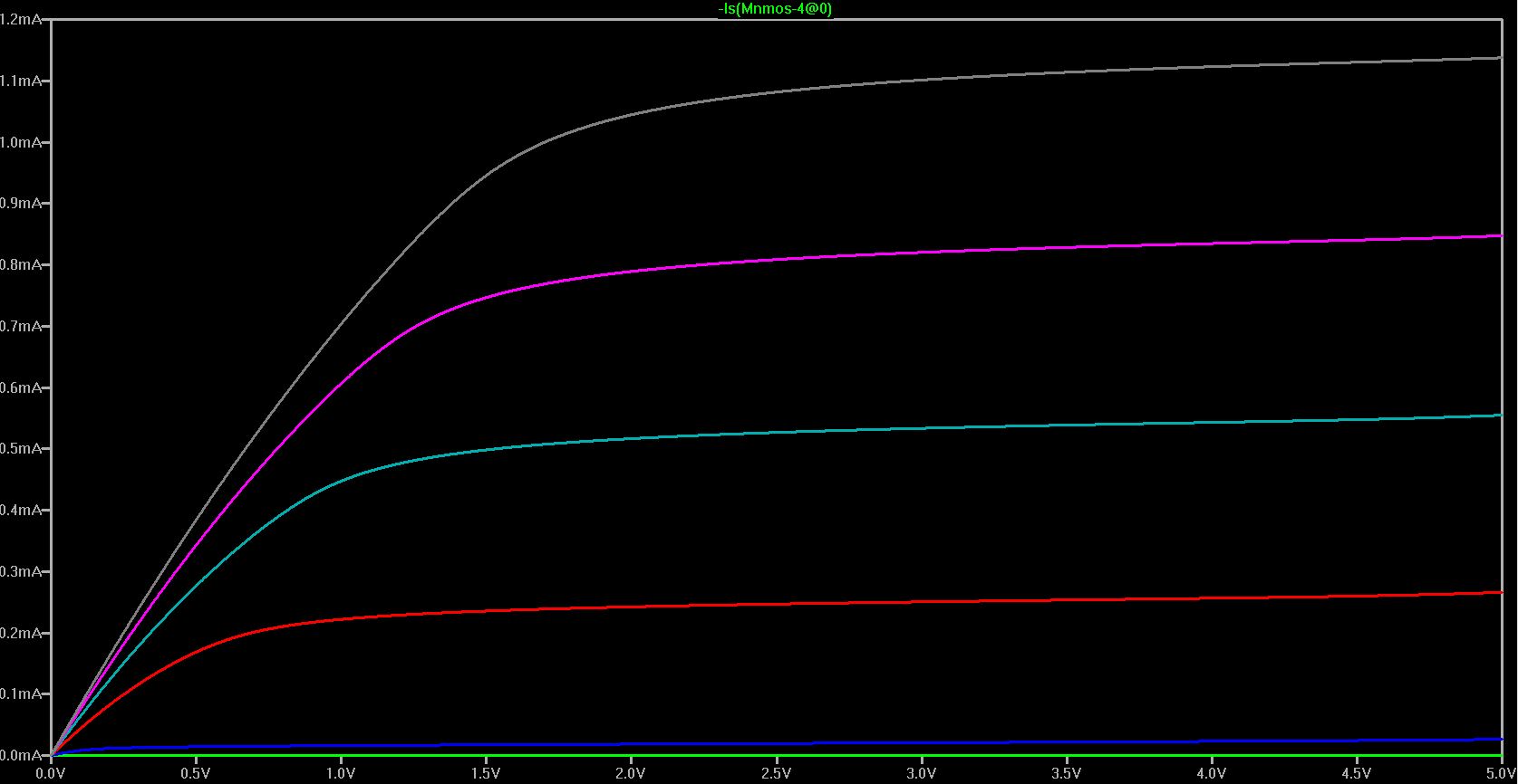
The wave form of the NMOS is as folloing
By going back to the NMOS schematic cell place the ground on it. Make sure to change the text size from 2 to .5
Next add wire Arcs to get the folloing.
Using Export >>> Create Export (or Better yet Ctrl+E) export the appropriate Pins to match the layout, see below;
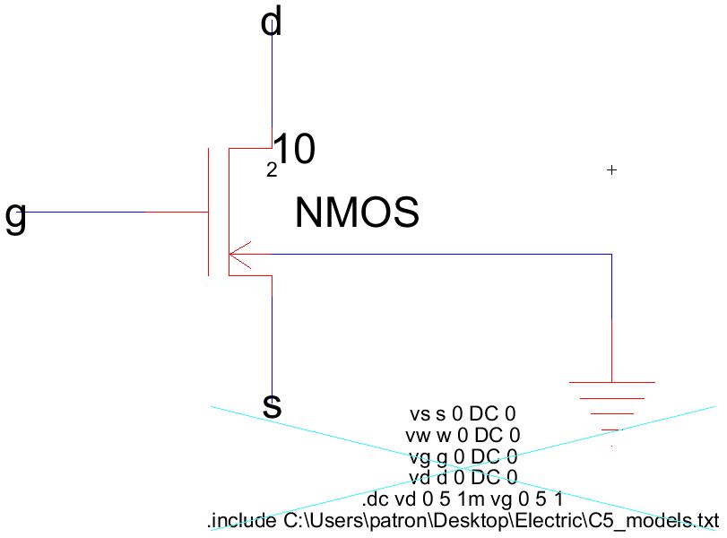
Change the MOS symboles and use the 3 terminal ones, set it to 10/2 for the characteristics.
Wave form for the above NMOS schematic. And this verifys that the lay out and the schematic wave form are the same.
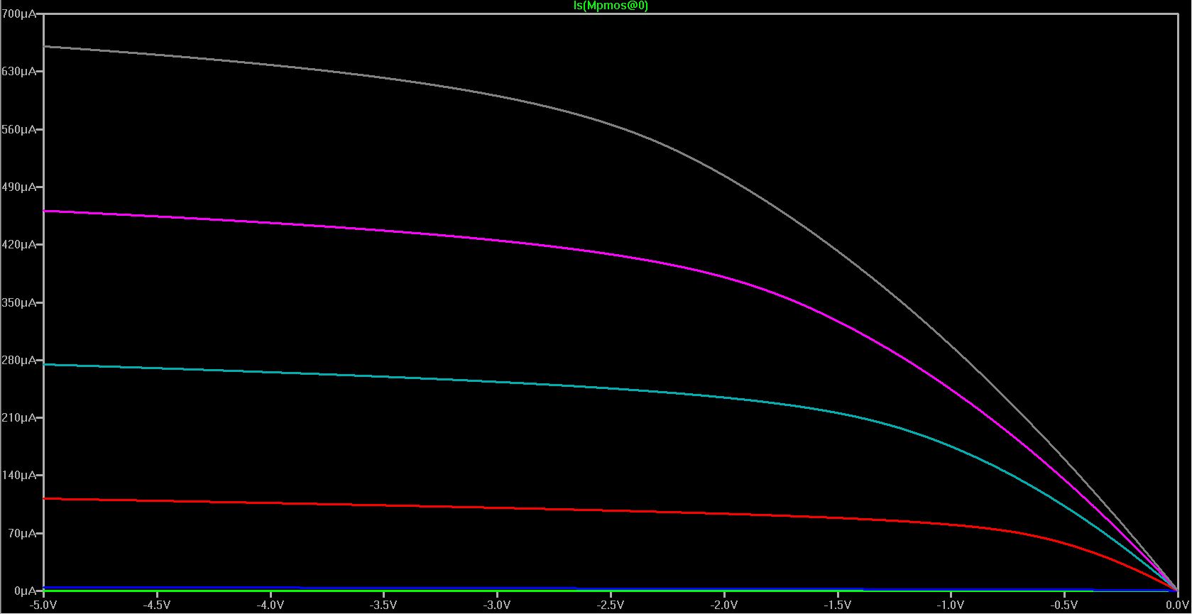
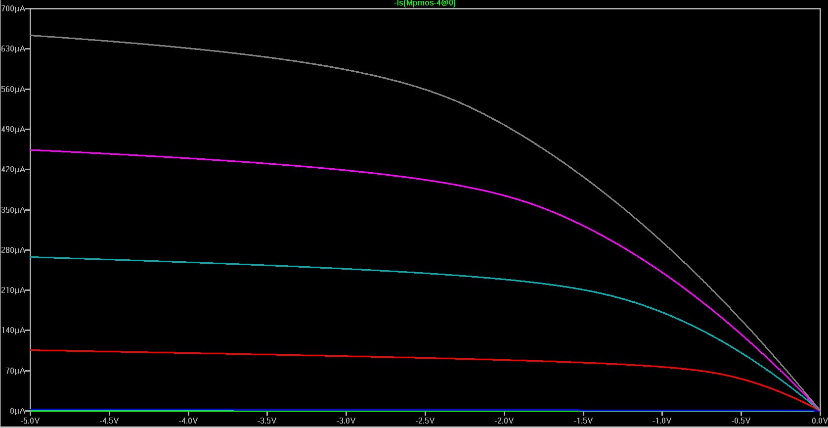
By folloing the same process to the PMOS, we get as the following fig.
Change the MOS symboles and use the 3 terminal ones, set it to 20/2 for the characteristics.
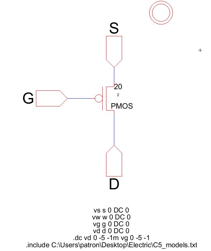
The wave form for the schematic form of PMOS. The wave form verifys that the lay out and the schematic results are the same;
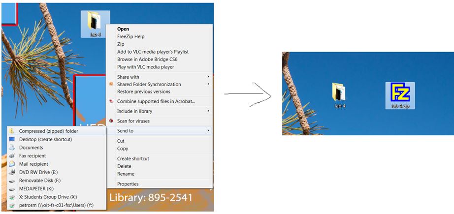
Finally, zip your file and send it to your e-mail, as the following fig.
.jelib file
Return to Labs
Return to students list