Lab 7 - ECE 421L
Authored
by Matt Mumm, mummm2@unlv.nevada.edu
Nov 1, 2013
Lab
description
Using buses and arrays in the design of 8bit inverters, muxs, and high-speed adders
Pre-lab:
Go through Tutorial 5 seen here.
Lab:
Create
a new lab and copy over your inverter (20/10) from a previous lab.
We are going to make an 8bit (8inputs and 8 outputs) inverter in
a much smaller schematic than usual. Create a new schematic cell and
drag the icon over. Rename the inverter inv[0:7]. By simply
naming the device this way, we are able to tell electric we want 8
inverters. The inverters are not connected in series or parallel.
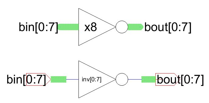
Notice the inputs and outputs have also been exported with names that have square brackets. 8 inputs and 8 outputs.
So bin[0] -> bout[0]. bin[1]->bout[1]. and so on...
The green line you see is a bus, multiple wires, all
connected to a single line. Buses enable us to specify a whole
series of inputs or outputs. But what if we want just the same
input to all 8 inputs? We can use the box with a J in it. This
allows the connection from a bus line to a wire line. Then we can
simply name the wire, not the node, say to Vin. Also notice
below the output bus has been named to out[0:7]. This means that
bus carries all 8 outputs.
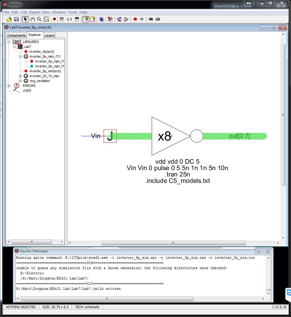
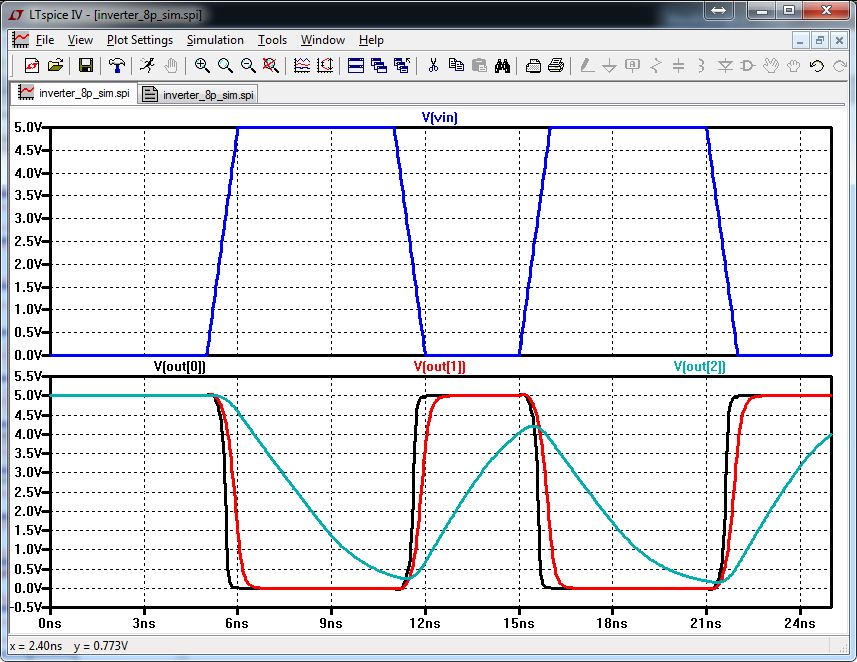
Lets do a simulation to see how a single input effects all 8 outputs through 8 inverters.
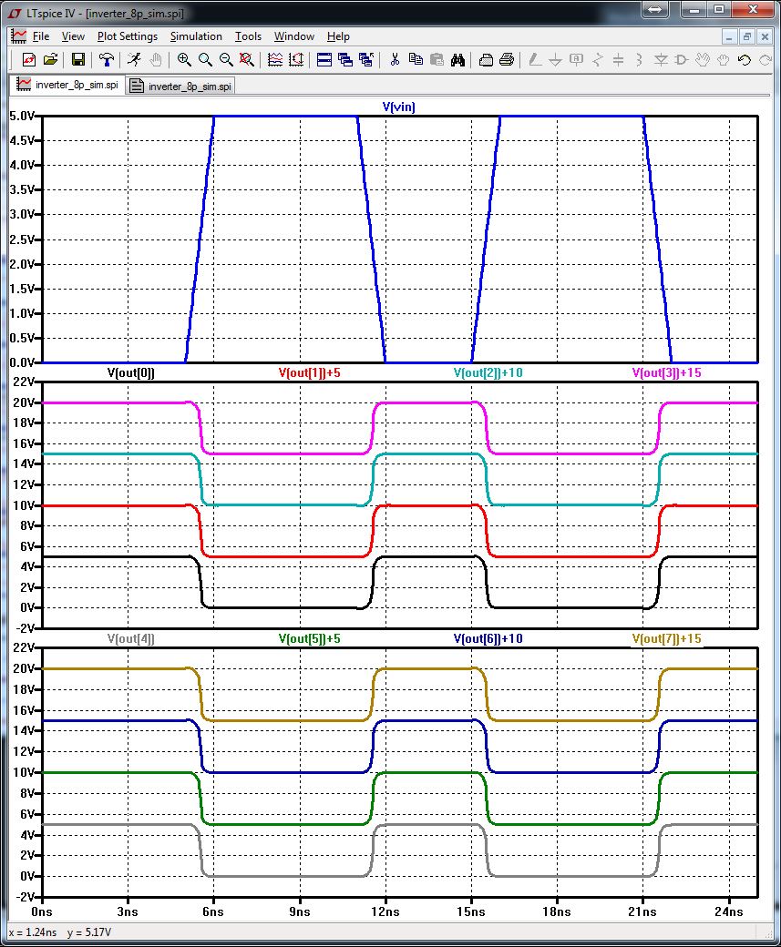
As you can see, all the outputs are the same. They have been manipulated in LTSpice so you can see them all.
Notice
there is a wire connected directly to the bus. This is ok if you
name the wire first to a specific output and then attach it to the bus.
Otherwise you will get an error. Such as, out[1].
Now we are going to check the delay of the inverter by adding different capacitor loads. 10f, 100f, 1p
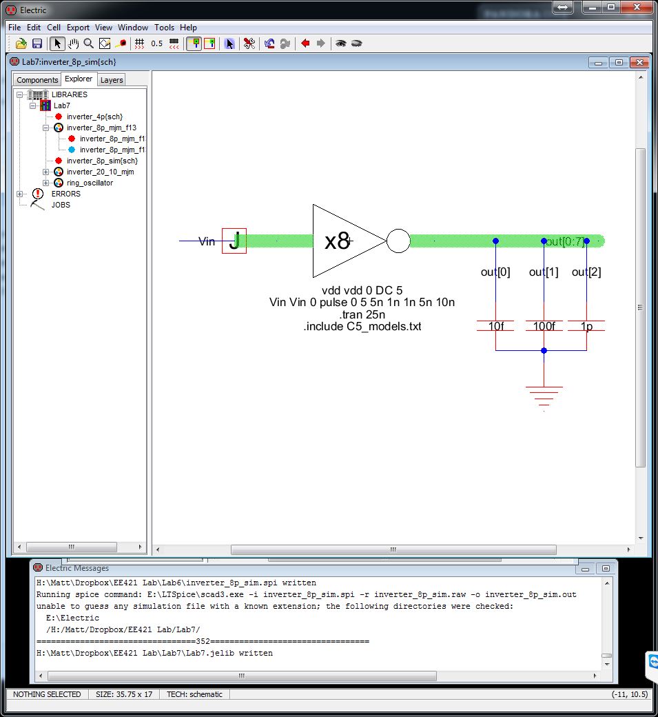
The delay is quite long with a 1pF load. The other 2 are not so bad.
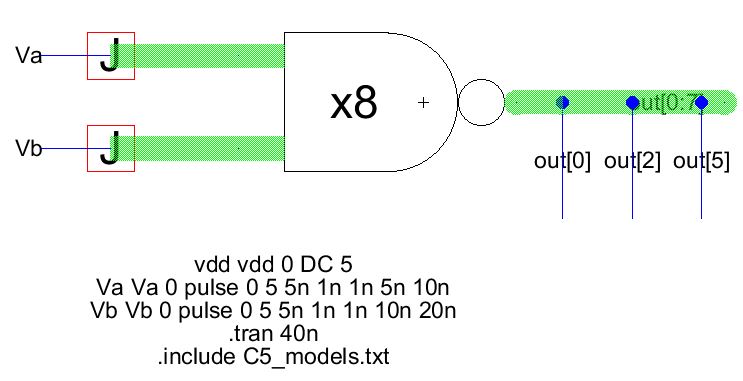
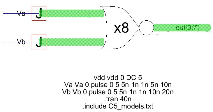
8bit NANDs, NORs, ANDs, ORs.
Here
I have repeated the same steps as above for different gates. I
have taken the icon for the simple 2 to 1 device, placed it in a new
schematic cell and added exports for 8 inputs (8 for A and 8 for B) and
8 outputs.
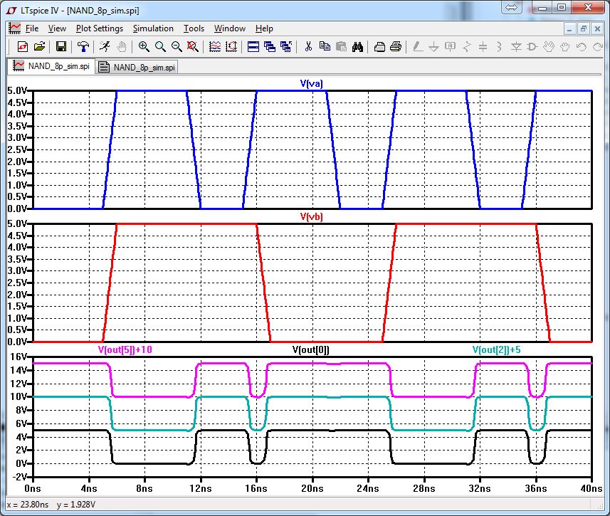
NAND:
NOR:
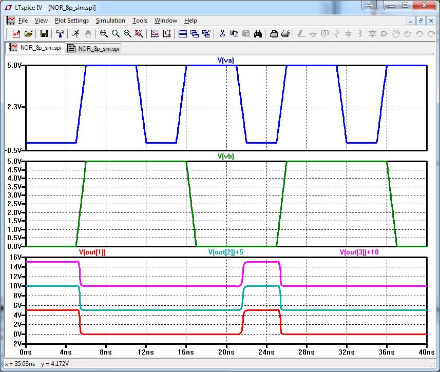
Notice for this simulation I did not place any wires on the output bus. I selected the outputs I wanted in LTSpice.
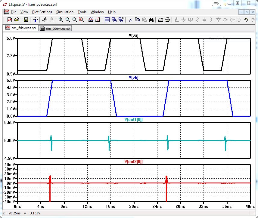
Now lets put 5 different devices together, simulate and took a look at the results.
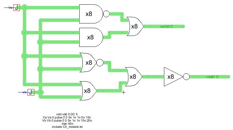
If
you do the logic behind the devices, the output of the first one will
always be high and the output of the second will always be low.
| A | B | A and B | A nand B | (AandB) or (AnandB) |
| 0 | 0 | 0 | 1 | 1 |
| 0 | 1 | 0 | 1 | 1 |
| 1 | 0 | 0 | 1 | 1 |
| 1 | 1 | 1 | 0 | 1 |
| A | B | A or B | A nor B | (AorB) or (AnorB) | [AorB) or (AnorB)]' |
| 0 | 0 | 0 | 1 | 1 | 0 |
| 0 | 1 | 1 | 0 | 1 | 0 |
| 1 | 0 | 1 | 0 | 1 | 0 |
| 1 | 1 | 1 | 0 | 1 | 0 |
The
spikes you see in the LTSpice simulation is a result from the pulse
changes and it takes time for the actual result to occur.
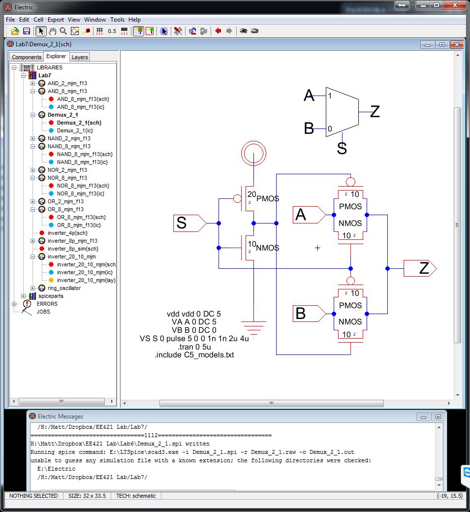
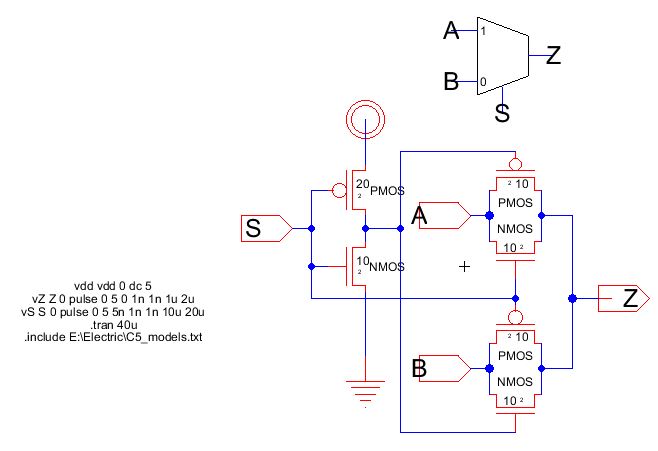
Now lets make a Multiplexer (Mux)
Remember
the object of a 2 to 1 mux is to take 2 inputs, select one of them and
output that result. This can be done by placing a NMOS and PMOS
together at the sources/drains. One of them will be the first
input (A) and the other is for the second (B). The outputs of
both will come together for the final output (Z). The selection
bit should use an inverter for both S and Si.
It is good to know
that NMOS is good at passing 0s, but not 1s. PMOS is good at
passing 1s, but not 0s. This is why we use a combination of both.
So that it does not matter whether A or B is high or low.
But how does this work?
Let
us ignore the PMOS for now. First lets set S, the selection bit, to
low; that makes Si, the inverted selection bit, high. Si will
turn on the NMOS connected to B. So the output on Z will be B. If
B is low, then the output will be low. However, if B is at VDD and so
is Si, then the NMOS is seen as off. Vgs=vg-vs=VDD-VDD=0. We need to
keep the NMOS on, so we will look at the other side of the NMOS as the
source. The minimum voltage needed to keep the NMOS on is Vthn.
So the source is actually at VDD-Vthn. Slightly below what
we want.
Now lets ignore the NMOS. Set B to high. S to
low, Si to high. So the PMOS is on and the output, Z, is B or
high or VDD. The same but opposite effect happens to the PMOS as the
NMOS if we set B to low or 0, it goes down to Vthp. This is why
we need the combination of NMOS and PMOS to pass a value to Z.
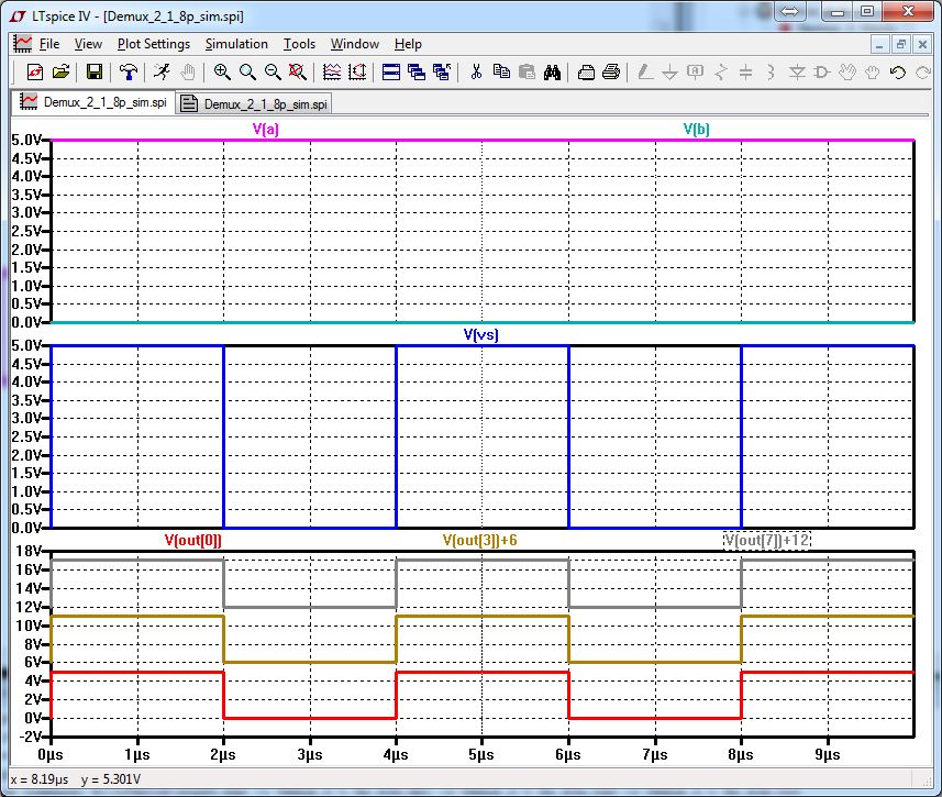
And simulate it.
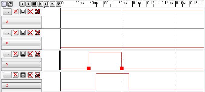
Notice the output changes depending on the selection bit.
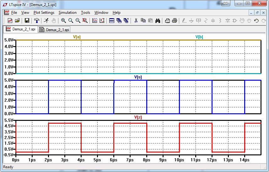
The same circuit can be used as a demultiplexer. All we have to do is change the input as Z and the outputs as A and B.
We can see that A takes the input as the selection is high. And B takes the input as selection is low.
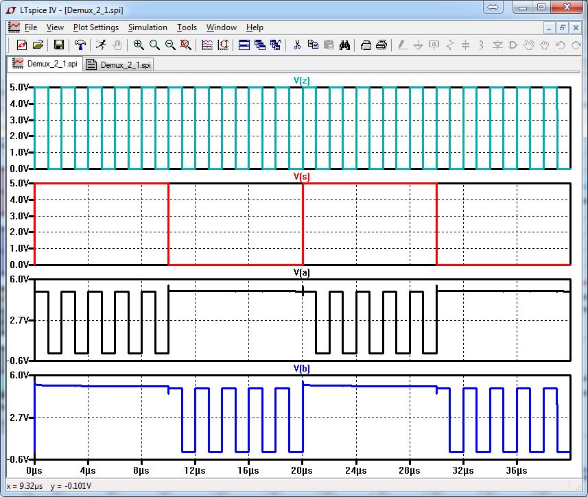
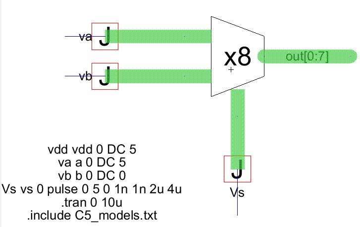
8bit mux
Repeat the same steps as for the inverter to create an 8 input and 8 output mux.
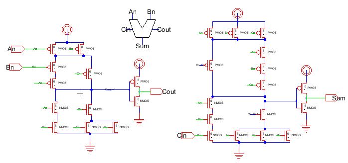
Finally,
lets make a full adder. Slightly different from the one in the
previous lab. We want NMOS, PMOS at 6/2. Following figure
12.20 in the CMOS book. This can been seen below.
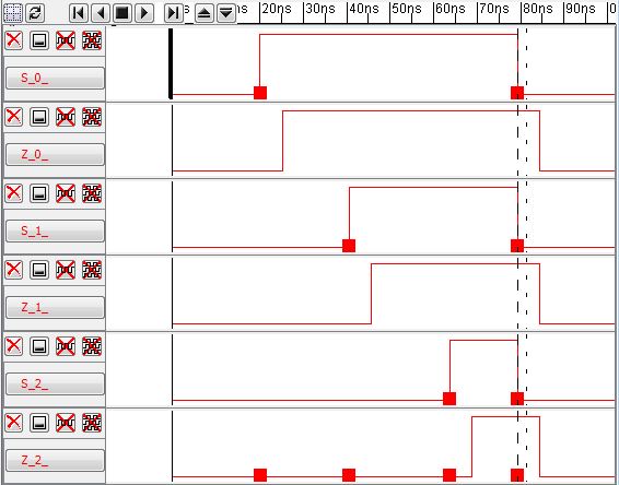
IRSIM Results
Now using the 2 input adder icon, we can create an 8 input adder with buses, as seen below. The inputs are the initial Cin, and then the carry outs of 0 to 6.
The outputs are Carry outs 0 to 7.
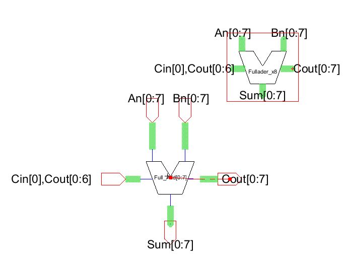
Layout
of the 8 input full adder. It is just 8 2 input adders connected
in series. The carry out of the first adder, goes to the carry in
of the next adder. This continues on throughout the circuit.
Each adder has its own A, B and Sum that is not connected to
another adder.

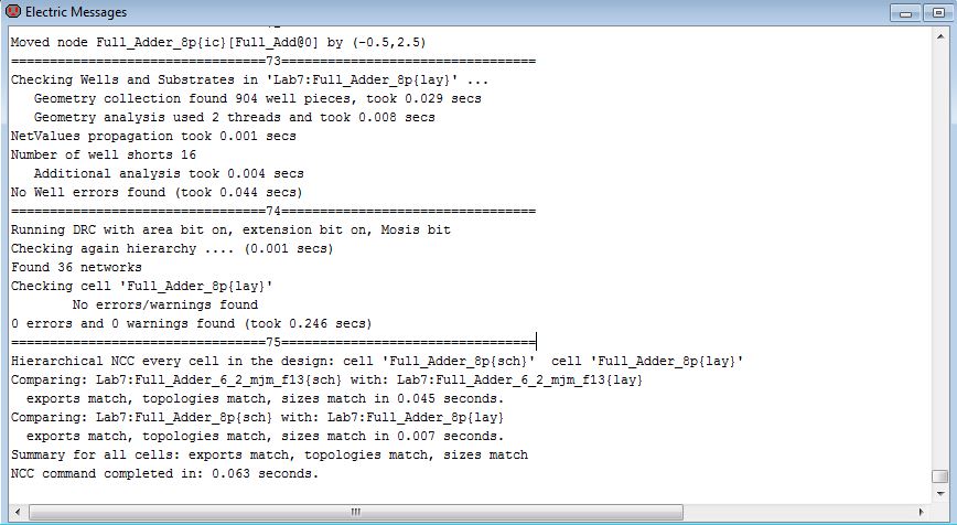
No errors are found.
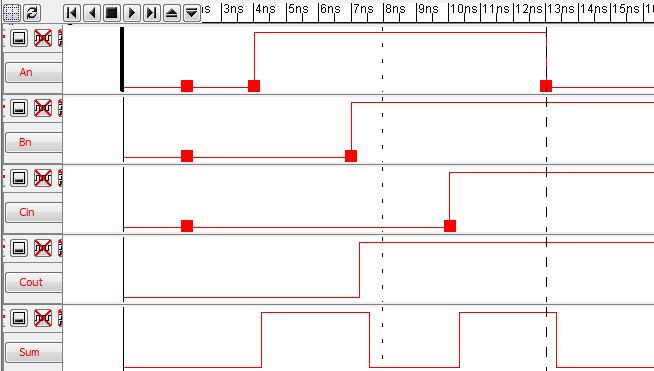
Finally a simulation showing the 8 input full adder works:
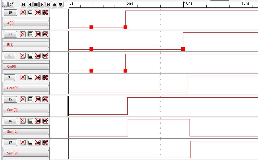
As cin[0] is set to high, the sum[0] is also set to high.
A[1]
is set to high, which causes sum[1] to go high, but then I set B[1] to
high later and sum[1] goes down while cout[1] goes up. The carry
out of 1 is the carry in of carry in of 2 which causes sum[2] to go up,
as it should.
My library file can be found here.
Be sure to backup your files. 
More information can be found at cmosedu.com